Zynq-7000 AP SoC and 7 Series FPGAs MIS v4.1 97
UG586 November 30, 2016
www.xilinx.com
Chapter 1: DDR3 and DDR2 SDRAM Memory Interface Solution
AXI4 Slave Interface Parameters
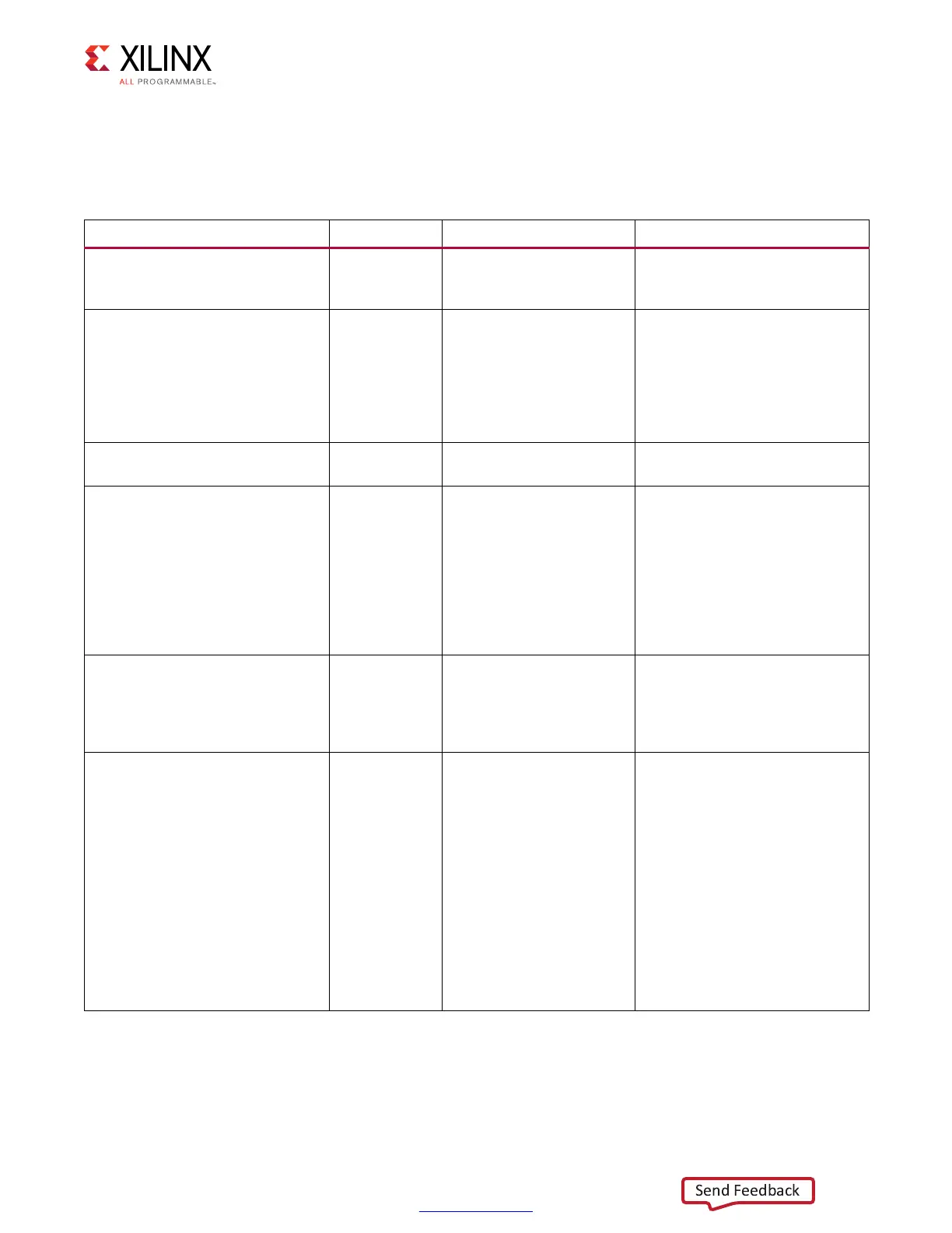
Table 1-19 lists the AXI4 slave interface parameters.
Table 1-19: AXI4 Slave Interface Parameters
Parameter Name Default Value Allowable Values Description
C_S_AXI_ADDR_WIDTH 32 32
This is the width of address read
and address write signals. This
value must be set to 32.
C_S_AXI_DATA_WIDTH 32 32, 64, 128, 256
This is the width of data signals;
a width of APP_DATA_WIDTH is
recommended for better
performance. Using a smaller
width invokes an Upsizer, which
would spend clocks in packing
the data.
C_S_AXI_ID_WIDTH 4 1–16
This is the width of ID signals for
every channel.
C_S_AXI_SUPPORTS_NARROW_
BURST
10, 1
This parameter adds logic
blocks to support narrow AXI
transfers. It is required if any
master connected to the
Memory Controller issues
narrow bursts. This parameter is
automatically set if the AXI data
width is smaller than the
recommended value.
C_RD_WR_ARB_ALGORITHM RD_PRI_REG
TDM, ROUND_ROBIN,
RD_PRI_REG,
RD_PRI_REG_STARVE_LIMI
T, WRITE_PRIORITY_REG,
WRITE_PRIORITY
This parameter indicates the
Arbitration algorithm scheme.
See Arbitration in AXI Shim,
page 100 for more information.
C_S_AXI_BASEADDR – Valid address
This parameter specifies the
base address for the memory
mapped slave interface. Address
requests at this address map to
rank 1, bank 0, row 0, column 0.
The base/high address together
define the accessible size of the
memory. This accessible size
must be a power of two.
Additionally, the base/high
address pair must be aligned to
a multiple of the accessible size.
The minimum accessible size is
4,096 bytes.
 Loading...


