Zynq-7000 AP SoC and 7 Series FPGAs MIS v4.1 248
UG586 November 30, 2016
www.xilinx.com
Chapter 1: DDR3 and DDR2 SDRAM Memory Interface Solution
Note: The tap variance across DQS byte groups is quite different due to fly-by routing.
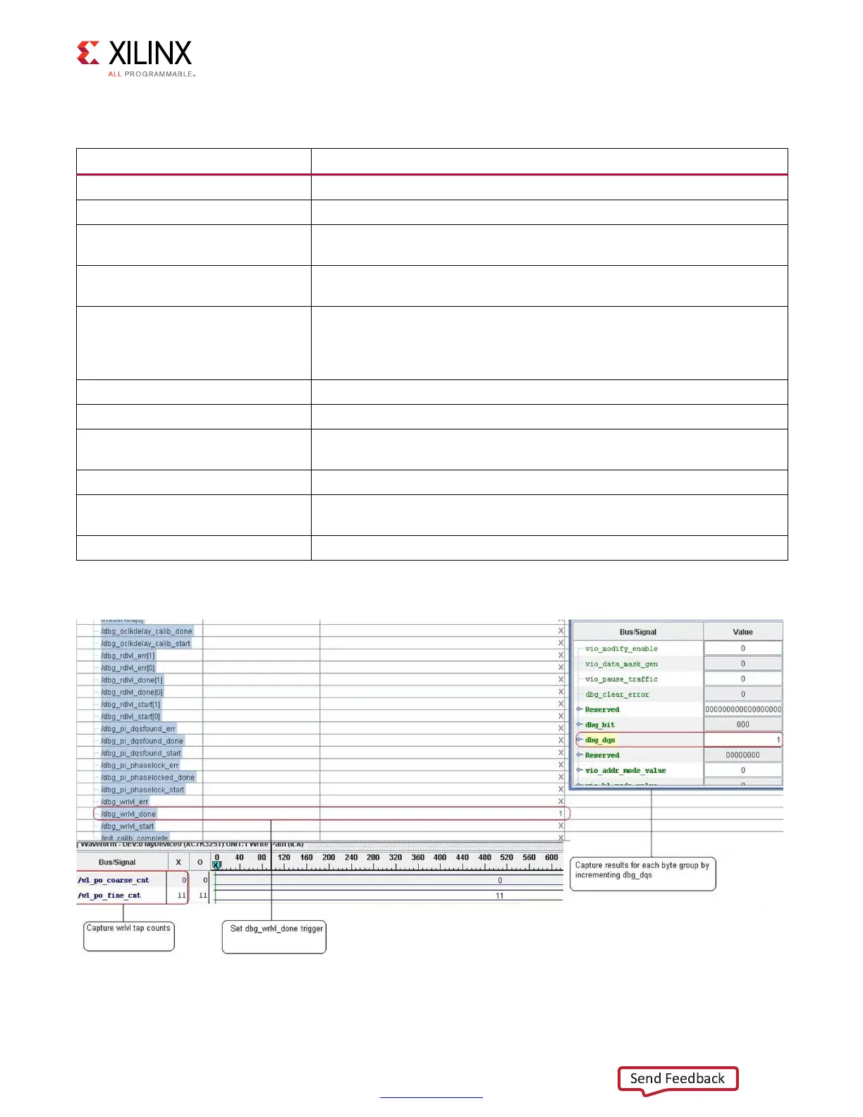
Expected Vivado Logic Analyzer Tool Results
Table 1-76: Debug Signals of Interest for Write Leveling Calibration
Signal Name Description
dbg_wrlvl_start Signifies the start of the Write Leveling stage of calibration.
dbg_wrlvl_done Signifies successful completion of the Write Leveling stage of calibration.
dbg_wrlvl_err
Signifies the Write Leveling stage of calibration exhibited errors and did
not complete.
wl_state_r
State variable for the Write Leveling State Machine. States can be decoded
in the ddr_phy_wrlvl.v module.
dbg_dqs_cnt_r
Signifies the DQS byte group being calibrated during Write Leveling. The
algorithm sequentially steps through the DQS byte groups until write
leveling completes successfully or a data byte group fails due a 0 to 1
transition not being detected on DQ.
dbg_wl_edge_detect_valid_r Signifies valid time Write Leveling algorithm is searching for edge.
dbg_rd_data_edge_detect_r_by_dqs Signifies Write Leveling calibration found the 0-to-1 edge transition.
dbg_wl_po_fine_cnt_by_dqs
PHASER_OUT Fine Taps found during Write Leveling. Byte capture based on
VIO dbg_dqs setting.
dbg_phy_wrlvl_128_75 PHASER_OUT Fine Taps found during Write Leveling.
dbg_wl_po_coarse_cnt_by_dqs
PHASER_OUT Coarse Taps found during Write Leveling. Byte capture based
on VIO dbg_dqs setting.
dbg_phy_wrlvl_155_129 PHASER_OUT Coarse Taps found during Write Leveling.
X-Ref Target - Figure 1-99
Figure 1-99: Trigger = dbg_wrlvl_done
 Loading...


