Zynq-7000 AP SoC and 7 Series FPGAs MIS v4.1 482
UG586 November 30, 2016
www.xilinx.com
Chapter 3: RLDRAM II and RLDRAM 3 Memory Interface Solutions
• Using the RLDRAM II/RLDRAM 3 physical layer to debug board-level issues
• General board-level debug techniques
The two primary issues encountered during verification of a memory interface are:
• Calibration not completing properly
• Data corruption during normal operation
Problems might be seen in simulation, hardware, or both due to various root causes.
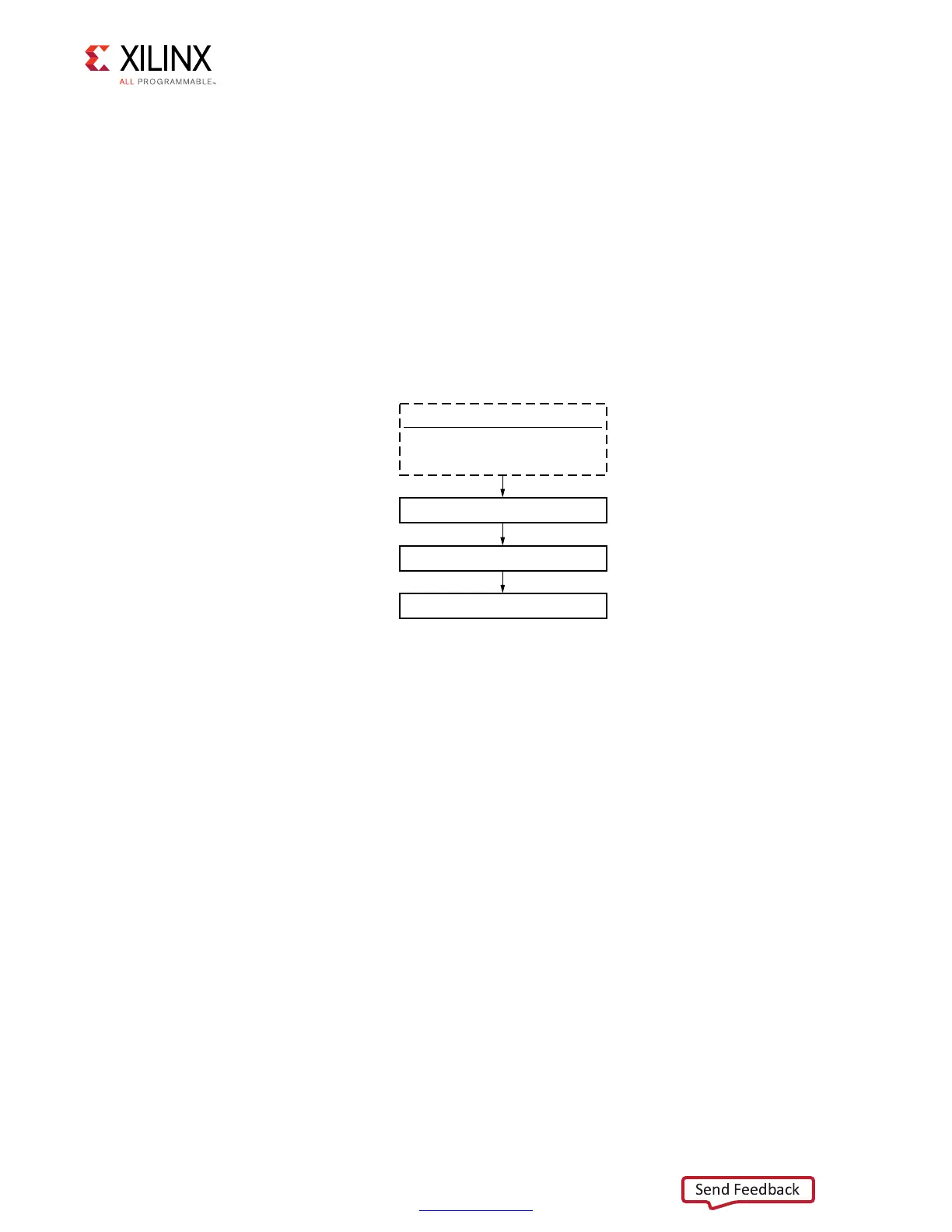
Figure 3-62 shows the overall flow for debugging problems associated with these two
general types of issues.
Debug Tools
Many tools are available to debug memory interface design issues. This section indicates
which resources are useful for debugging a given situation.
Example Design
RLDRAM II/RLDRAM 3 design generation using the MIG tool produces an example design
and a user design. The example design includes a synthesizable test bench that has been
fully verified in simulation and hardware. This design can be used to observe the behavior
of the MIG tool design and can also aid in identifying board-related problems.
Debug Signals
The MIG tool includes a Debug Signals Control option on the FPGA Options screen.
Enabling this feature allows calibration, tap delay, and read data signals to be monitored
using the Vivado logic analyzer feature. Selecting this option port maps the debug signals
to VIO modules of the Vivado logic analyzer feature in the design top module.
X-Ref Target - Figure 3-62
Figure 3-62: RLDRAM II/RLDRAM 3 MIG Tool Debug Flowchart
3YMPTOMSIN3IMULATION(ARDWARE
#ALIBRATION&AILURE
$ATA"IT"YTE#ORRUPTION%RRORS
3IMULATION$EBUG
3YNTHESIS)MPLEMENTATION$EBUG
(ARDWARE$EBUG
 Loading...


