Zynq-7000 AP SoC and 7 Series FPGAs MIS v4.1 669
UG586 November 30, 2016
www.xilinx.com
Appendix A
General Memory Routing Guidelines
1. Include package delay in routing constraints when determining signal trace lengths.
When minimum and maximum values are available for the package delay, use the
midpoint between the minimum and maximum values.
2. DQ and DQS signals in the same byte should be routed in the same layer from FPGA to
DRAM, except in the breakout areas.
3. For fly-by routing, address, command, control, and clock signals can be routed on
different layers but each signal needs to be routed consistently in one layer across all
DRAMs. Any signal layer switching via needs to have one ground via within a 50 mil
perimeter range.
4. Ensure the memory ODT settings match transmission line impedance.
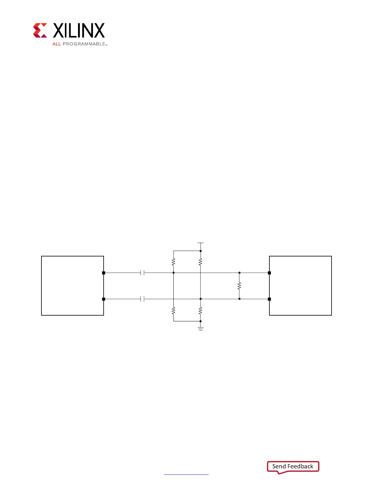
5. ck as shown in Figure A-1.
X-Ref Target - Figure A-1
Figure A-1: System Clock
UG583_c2_57_060315
CLOCK
GENERATOR
FPGA
GND
SYSCLK_C_N
SYSCLK_C_P
SYSCLK_N
SYSCLK_P
C650
0.1 µF
25V
XSR
R594
1.00K
1/16W
1%
R596
1.00K
1/16W
1%
R595
1.00K
1/16W
1%
R692
100K
1/10W
1%
R597
1.00K
1/16W
1%
C651
0.1 µF
25V
XSR
12
12
VCC1V2_FPGA
1
2
1
2
1
2
1
2
1
2
 Loading...


