Zynq-7000 AP SoC and 7 Series FPGAs MIS v4.1 319
UG586 November 30, 2016
www.xilinx.com
Chapter 2: QDR II+ Memory Interface Solution
The client interface (also known as the user interface) uses a protocol based entirely on
single data rate (SDR) signals to make read and write requests. For more details about this
protocol, see the User Interface section. The physical interface generating the proper timing
relationships and DDR signaling to communicate with the external memory device, while
conforming to QDR II+ protocol and timing requirements. For more information, see the
Physical Interface section.
Within the PHY, logic is broken up into read and write paths. The read path is responsible
for calibration and providing read responses back to you with a corresponding valid signal.
For more details about this process, see the Calibration section. The write path generates
the QDR II+ signaling for generating read and write requests. This includes control signals,
address, data, and byte writes.
User Interface
The client interface connects the 7 series FPGA user design to the QDR II+ SRAM solutions
core to simplify interactions between you and the external memory device.
Command Request Signals
The client interface provides a set of signals used to issue a read or write command to the
memory device. These signals are summarized in Table 2-7. To accommodate for burst
length four devices, the client interface contains ports for two read and two write
transactions. When using burst length four, only the ports ending in zero should be used.
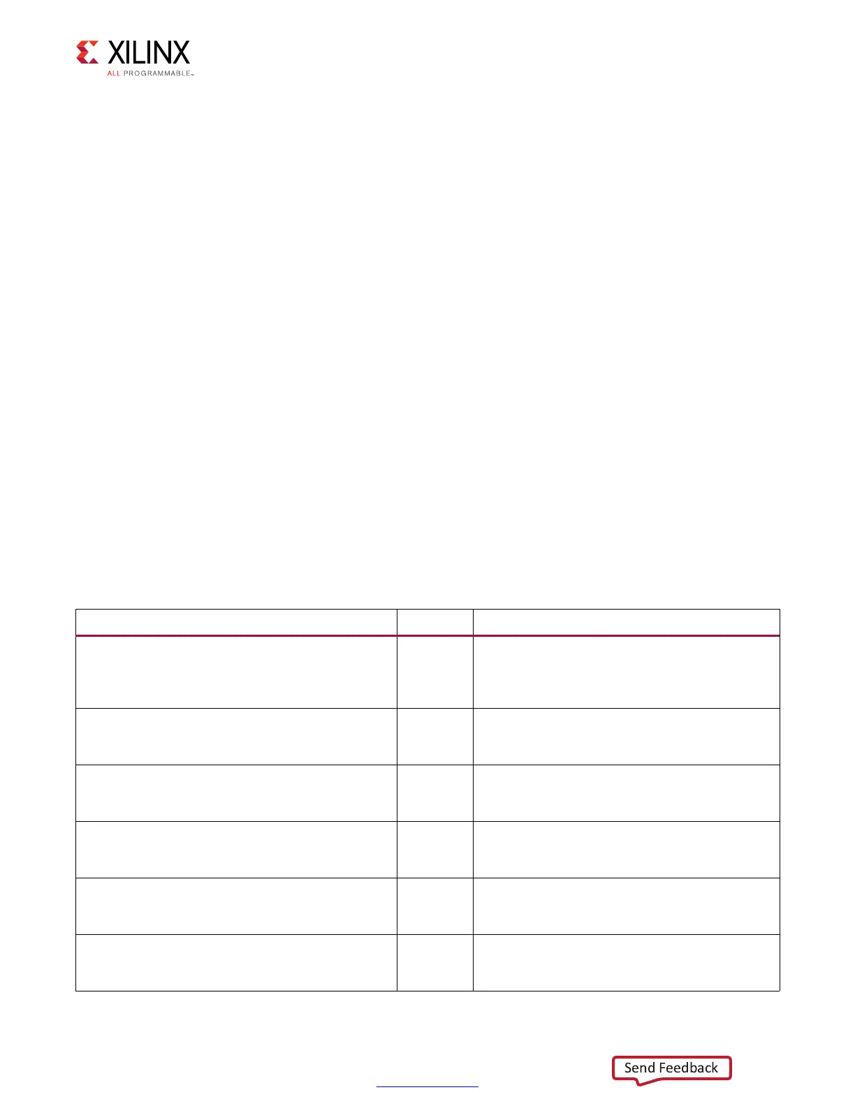
Table 2-7: Client Interface Request Signals
Signal Direction Description
init_calib_complete Output
Calibration Done. This signal indicates to the
user design that read calibration is complete
and you can now initiate read and write
requests from the client interface.
app_rd_addr0[ADDR_WIDTH – 1:0] Input
Read Address. This bus provides the address to
use for a read request. It is valid when
app_rd_cmd0 is asserted.
app_rd_cmd0 Input
Read Command. This signal is used to issue a
read request and indicates that the address on
port 0 is valid.
app_rd_data0[DATA_WIDTH × BURST_LEN – 1:0] Output
Read Data. This bus carries the data read back
from the read command issued on
app_rd_cmd0.
app_rd_valid0 Output
Read Valid. This signal indicates that data read
back from memory is now available on
app_rd_data0 and should be sampled.
app_rd_addr1[ADDR_WIDTH – 1:0] Input
Read Address. This bus provides the address to
use for a read request. It is valid when
app_rd_cmd1 is asserted.
 Loading...


