Zynq-7000 AP SoC and 7 Series FPGAs MIS v4.1 35
UG586 November 30, 2016
www.xilinx.com
Chapter 1: DDR3 and DDR2 SDRAM Memory Interface Solution
IMPORTANT: The Data Mask (DM) option is always selected for AXI designs and is grayed out (you
cannot select it). For AXI interfaces, Read Modify Write (RMW) is supported and for RMW to mask
certain bytes of Data Mask bits should be present. Therefore, the DM is always enabled for AXI interface
designs. This is the case for all data widths except 72-bit.
For 72-bit interfaces, Error Correcting Code (ECC) is enabled and DM is deselected and grayed out. If
DM is enabled for 72-bit designs, computing ECC is not compatible, therefore DM is disabled for 72-bit
designs.
• Number of Bank Machines – The list shows the number of bank machines that are
supported for the selected design configuration.
• Ordering – This feature allows the Memory Controller to reorder commands to
improve the memory bus efficiency.
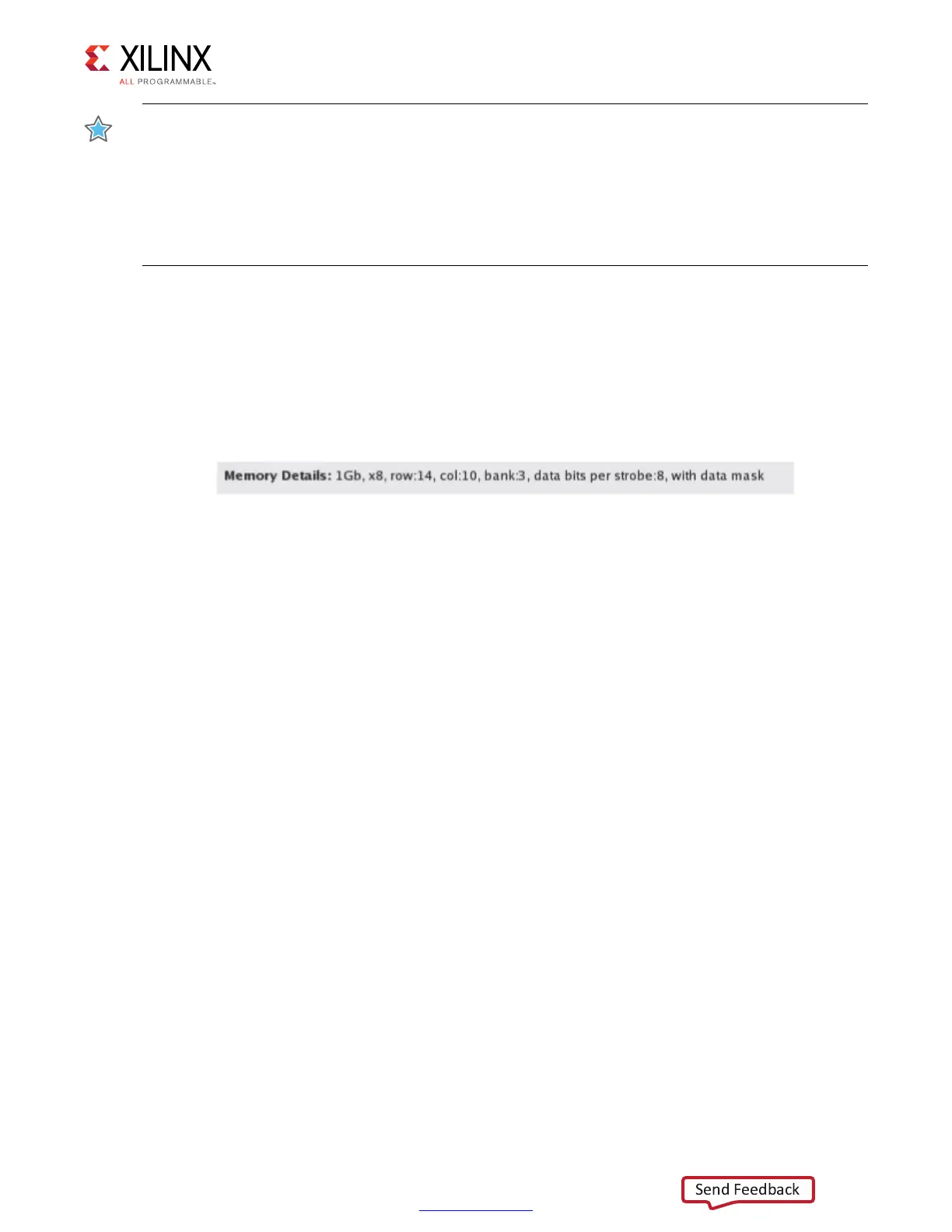
• Memory Details – The bottom of the Controller Options page (Figure 1-17) displays
the details for the selected memory configuration (Figure 1-18).
Create Custom Part
1. On the Controller Options page select the appropriate frequency. Either use the spin
box or enter a valid value using the keyboard. Values entered are restricted based on the
minimum and maximum frequencies supported.
2. Select the appropriate memory part from the list. If the required part or its equivalent is
unavailable, a new memory part can be created. To create a custom part, click the
Create Custom Part below the Memory Part pull-down menu. A new page appears, as
shown in Figure 1-19.
X-Ref Target - Figure 1-18
Figure 1-18: Memory Details
 Loading...


