Zynq-7000 AP SoC and 7 Series FPGAs MIS v4.1 261
UG586 November 30, 2016
www.xilinx.com
Chapter 1: DDR3 and DDR2 SDRAM Memory Interface Solution
Debugging PRBS Read Leveling Failures
Calibration Overview
This stage of calibration was added in MIG 7 series v1.7 and determines the read data valid
window using complex pattern that is written once and read back from the DDR3 SDRAM.
Debug
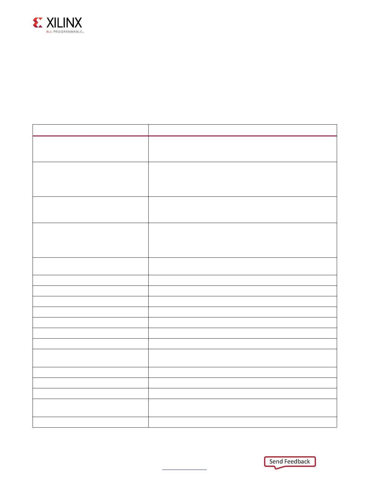
Table 1-81: Debug Signals of Interest for PRBS Read Leveling Calibration
Debug Signal Signal Description
left_edge_pb
Signifies PHASER_IN fine tap value of starting valid read window (left
edge) for each bit in a byte. left_edge_pb[5:0] is the left edge of Bit[0]
and left_edge_pb[47:42] is the left edge of Bit[7].
left_loss_pb
Signifies the loss in aggregate window size caused by left edge
change for each bit in a byte. If left edge change of the bit does not
affect the valid window, it is set to "0," left_loss_pb[1:0] is for Bit[0],
and left_loss_pb[15:14] is for Bit[7].
right_edge_pb
Signifies PHASER_IN fine tap value of ending valid read window (right
edge) for each bit in a byte. right_edge_pb[5:0] is right edge of Bit[0]
and right_edge_pb[47:42] is the right edge of Bit[7].
right_gain_pb
Signifies the gain in aggregate valid window caused by right edge
change for each bit in a byte. If right edge change of the bit does not
affect the valid window, it is set to "0," right_gain_pb[1:0] is for Bit[0],
and right_gain_pb[15:14] is for Bit[7].
prbs_dqs_cnt_r
Signifies the current DQS byte group being calibrated during PRBS
Read Leveling. Use VIO dbg_dqs to select the byte group.
prbs_rdlvl_start Signifies the start of PRBS Read Leveling calibration.
prbs_rdlvl_done Signifies the successful completion of PRBS Read Leveling.
compare_err_r0 Signifies data mismatch on first rising edge data comparison.
compare_err_r1 Signifies data mismatch on second rising edge data comparison.
compare_err_r2 Signifies data mismatch on third rising edge data comparison.
compare_err_r3 Signifies data mismatch on forth rising edge data comparison.
compare_err_f0 Signifies data mismatch on first falling edge data comparison.
compare_err_f1 Signifies data mismatch on second falling edge data comparison.
compare_err_f2 Signifies data mismatch on third falling edge data comparison.
compare_err_f3 Signifies data mismatch on forth falling edge data comparison.
compare_err Signifies data comparison failure due to a read data pattern
prbs_dqs_tap_cnt_r
Signifies the internal counter which tracks PHASER_IN fine tap
movement.
pi_counter_read_val Signifies DQS PHASER_IN fine tap setting.