Zynq-7000 AP SoC and 7 Series FPGAs MIS v4.1 374
UG586 November 30, 2016
www.xilinx.com
Chapter 2: QDR II+ Memory Interface Solution
Write Init Debug Signals
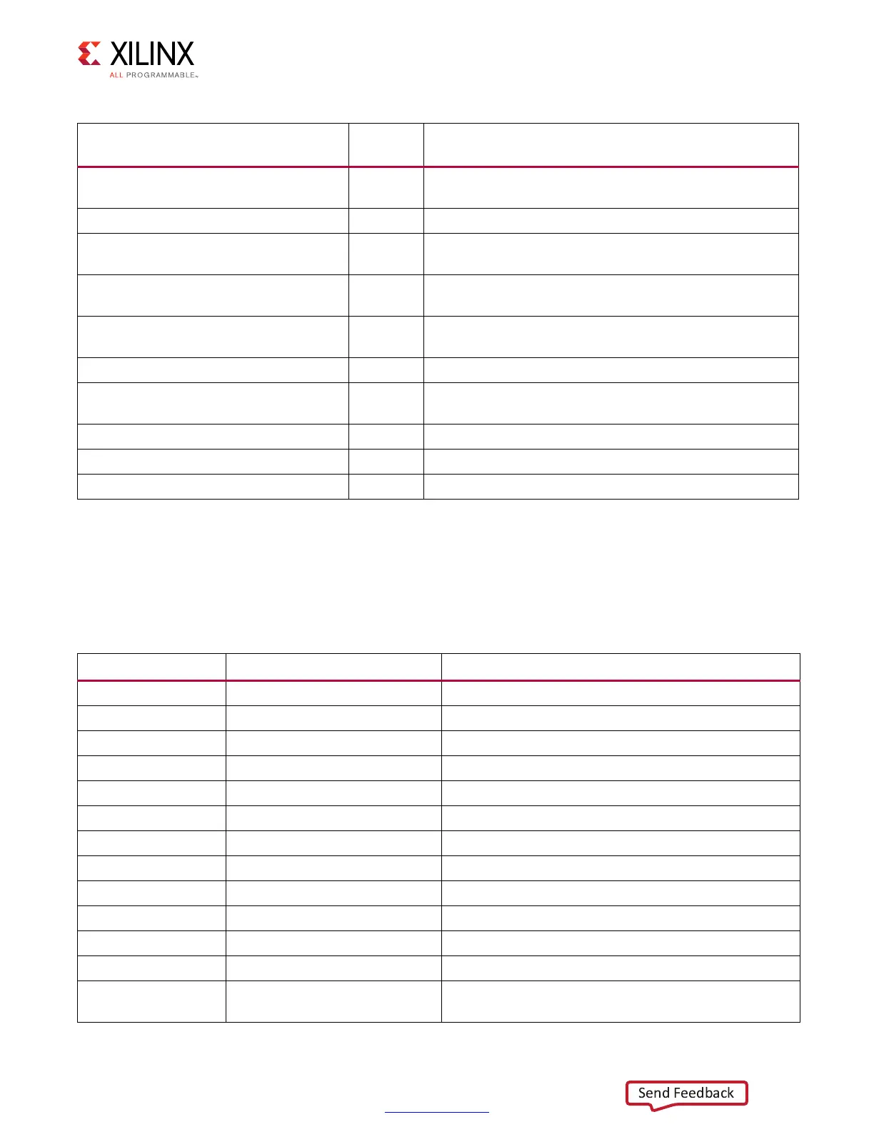
Table 2-19 indicates the mapping between the write init debug signals on the
dbg_wr_init bus and debug signals in the PHY. All signals are found within the
qdr_phy_write_init_sm module and are all valid in the clk domain.
dbg_error_adj_latency Output
This signal indicates that the target PHY_LATENCY could
not be achieved
dbg_align_rd0 [DATA_WIDTH – 1:0] Output This bus shows the captured output of the first rising data
dbg_align_rd1 [DATA_WIDTH – 1:0] Output
This bus shows the captured output of the second rising
data
dbg_align_fd0 [DATA_WIDTH – 1:0] Output
This bus shows the captured output of the first falling
data
dbg_align_fd1 [DATA_WIDTH – 1:0] Output
This bus shows the captured output of the second falling
data
dbg_cmplx_rd_loop Input When High, complex read level continues forever.
dbg_cmplx_rd_lane[2:0] Input
Selects the lane to hang on when dbg_cmplx_rd_loop ==
'b1.
dbg_K_left_shift_right Input Shifts the location of the left edge sent to the POC right.
dbg_K_right_shift_left Input Shifts the location of the right edge sent to the POC left.
dbg_cmplx_wr_loop Input When High, complex write pattern is written indefinitely.
Table 2-18: DEBUG_PORT Signal Descriptions (Cont’d)
Signal Direction Description
Table 2-19: Write Init Debug Signal Map
Bits PHY Signal Name Description
dbg_wr_init[14:0] phy_init_r One hot state machine.
dbg_wr_init[18:15] phase_valid Per byte lane comparison results.
dbg_wr_init[22:19] lanes_solid_r Comparison success post threshold per lane.
dbg_wr_init[23] po_delay_done Phaser out adjustment complete.
dbg_wr_init[24] rdlvl_stg1_done Read level cycle complete.
dbg_wr_init[25] rdlvl_stg1_start Start read level calibration.
dbg_wr_init[26] edge_adv_cal_start Start cycle (edge) alignment.
dbg_wr_init[27] edge_adv_cal_done Edge alignment complete.
dbg_wr_init[28] cal_stage2_start Start latency calibration.
dbg_wr_init[29] read_cal_done Latency calibration complete.
dbg_wr_init[30] rst_stg1_r Reset read level block.
dbg_wr_init[31] rst_stg2_r Reset edge and latency calibration logic.
dbg_wr_init[32] suppress_stg1
All bytes successfully read leveled. Suppress further
read levels.
 Loading...


