Zynq-7000 AP SoC and 7 Series FPGAs MIS v4.1 231
UG586 November 30, 2016
www.xilinx.com
Chapter 1: DDR3 and DDR2 SDRAM Memory Interface Solution
Reference Boards
Various Xilinx development boards support MIG IP core that include FPGA interfaces to a
DDR SODIMM. These boards can be used to prototype designs and establish that the core
can communicate with the system.
• 7 series FPGA evaluation boards
°
VC707
°
KC705
°
AC701
Hardware Debug
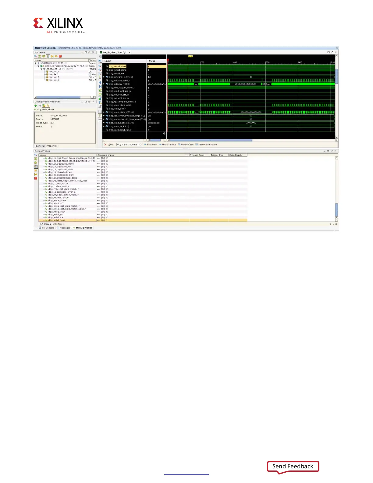
Hardware issues can range from calibration failures to issues seen after hours of testing.
This section provides debug steps for common issues. The Vivado logic analyzer feature is
a valuable resource to use in hardware debug. The signal names mentioned in the following
individual sections can be probed using the Vivado logic analyzer feature for debugging
the specific issues.
X-Ref Target - Figure 1-96
Figure 1-96: Vivado Analyzer Feature
 Loading...


