EasyManua.ls Logo

Xilinx Zynq-7000 User Manual

Xilinx Zynq-7000
678 pages
To Next Page IconTo Next Page
To Previous Page IconTo Previous Page
Page #557 background imageLoading...
Page #557 background image
Zynq-7000 AP SoC and 7 Series FPGAs MIS v4.1 557
UG586 November 30, 2016
www.xilinx.com
Chapter 4: LPDDR2 SDRAM Memory Interface Solution
Traffic Generator Operation
The traffic generator module contained within the synthesizable test bench can be
parameterized to create various stimulus patterns for the memory design. It can produce
repetitive test patterns for verifying design integrity as well as pseudo-random data
streams that model real-world traffic.
You can define the address range through the BEGIN_ADDRESS and END_ADDRESS
parameters. The Init Memory Pattern Control block directs the traffic generator to step
sequentially through all the addresses in the address space, writing the appropriate data
value to each location in the memory device as determined by the selected data pattern. By
default, the test bench uses the address as the data pattern, but the data pattern in this
example design can be modified using vio_data_mode signals that can be modified
within the Vivado logic analyzer feature.
When the memory has been initialized, the traffic generator begins stimulating the user
interface port to create traffic to and from the memory device. By default, the traffic
generator sends pseudo-random commands to the port, meaning that the instruction
sequences (R/W, R, W) and addresses are determined by PRBS generator logic in the traffic
generator module.
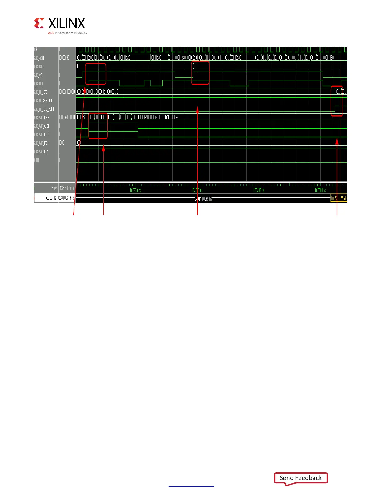
X-Ref Target - Figure 4-38
Figure 4-38: User Interface Read and Write Cycle
Send Feedback

Table of Contents

Other manuals for Xilinx Zynq-7000

Question and Answer IconNeed help?

Do you have a question about the Xilinx Zynq-7000 and is the answer not in the manual?

Xilinx Zynq-7000 Specifications

General IconGeneral
SeriesZynq-7000
Number of CoresDual-core
Processor SpeedUp to 1 GHz
Device TypeSoC
Logic CellsUp to 350K
DSP SlicesUp to 900
External Memory InterfacesDDR3, DDR2, LPDDR2
I/O StandardsLVCMOS, HSTL, SSTL
Operating Temperature-40°C to +100°C (Industrial), 0°C to +85°C (Commercial)
Package OptionsVarious BGA packages
I/O Voltage3.3V

Summary

Chapter 1: DDR3 and DDR2 SDRAM Memory Interface Solution

Introduction

Overview of the DDR3 and DDR2 SDRAM Memory Interface Solution, its architecture, and features.

Features

Highlights enhancements in 7 series FPGA memory interface solutions over earlier families.

Chapter 2: QDR II+ Memory Interface Solution

Introduction

Details the QDR II+ SRAM Memory Interface Solution, its architecture, and usage.

Chapter 3: RLDRAM II and RLDRAM 3 Memory Interface Solutions

Introduction

Explains RLDRAM II/III Memory Interface Solutions, covering architecture, usage, and simulation.

Chapter 4: LPDDR2 SDRAM Memory Interface Solution

Introduction

Introduces the LPDDR2 SDRAM Memory Interface Solution, its core components, and features.

Features

Details enhancements in LPDDR2 SDRAM solutions, including performance and hardware blocks.

Chapter 5: Multicontroller Design

Introduction

Describes specifications, supported features, and pinout rules for multicontroller designs.

Chapter 6: Upgrading the ISE/CORE Generator MIG Core in Vivado

Appendix A: General Memory Routing Guidelines

Related product manuals