Zynq-7000 AP SoC and 7 Series FPGAs MIS v4.1 581
UG586 November 30, 2016
www.xilinx.com
Chapter 4: LPDDR2 SDRAM Memory Interface Solution
User Interface Block
The UI block presents the UI to a user design. It provides a simple alternative to the native
interface. The UI block:
• Buffers read and write data
• Reorders read return data to match the request order
• Presents a flat address space and translates it to the addressing required by the SDRAM
Native Interface
The native interface connects to an FPGA user design to allow access to an external memory
device.
Command Request Signals
The native interface provides a set of signals that request a read or write command from the
Memory Controller to the memory device. These signals are summarized in Table 4-16.
The bank, row, and column comprise a target address on the memory device for read and
write operations. Commands are specified using the cmd[2:0] input to the core. The
available read and write commands are shown in Table 4-17.
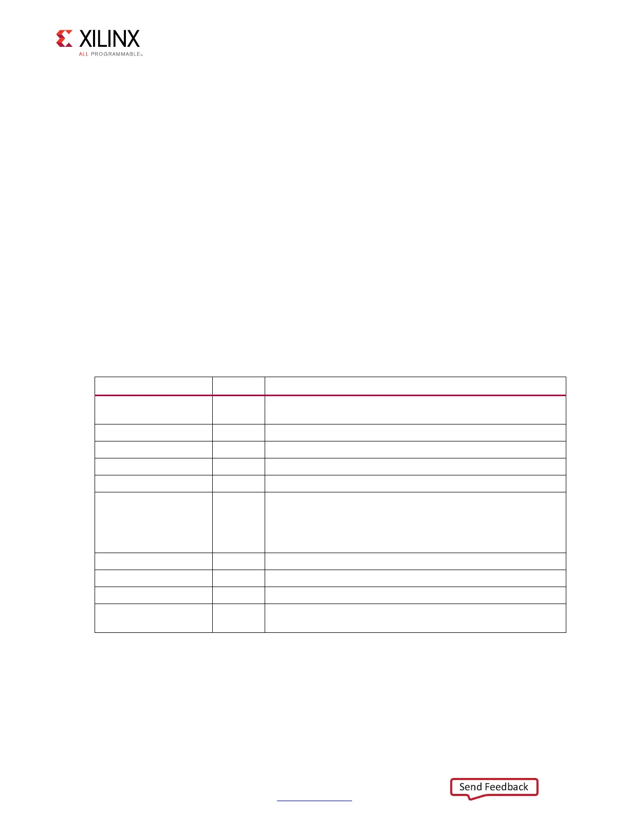
Table 4-16: Native Interface Command Signals
Signal Direction Description
accept Output
This output indicates that the memory interface accepts the
request driven on the last cycle.
bank[2:0] Input This input selects the bank for the current request.
bank_mach_next[] Output This output is reserved and should be left unconnected.
cmd[2:0] Input This input selects the command for the current request.
col[COL_WIDTH – 1:0] Input This input selects the column address for the current request.
data_buf_addr[7:0] Input
This input indicates the data buffer address where the Memory
Controller:
Locates data while processing write commands.
Places data while processing read commands.
hi_priority Input This input is reserved and should be connected to logic 0.
rank[] Input This input is reserved and should be connected to logic 0.
row[ROW_WIDTH – 1:0] Input This input selects the row address for the current request.
use_addr Input
The user design strobes this input to indicate that the request
information driven on the previous state is valid.
 Loading...


