Zynq-7000 AP SoC and 7 Series FPGAs MIS v4.1 447
UG586 November 30, 2016
www.xilinx.com
Chapter 3: RLDRAM II and RLDRAM 3 Memory Interface Solutions
Calibration
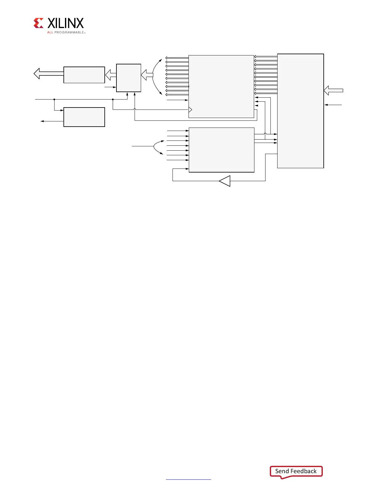
The calibration logic includes providing the required amount of delay on the read clock and
read data to align the clock in the center of the data valid window. The centering of the
clock is done using PHASERs, which provide very fine resolution delay taps on the clock.
Each PHASER_IN fine delay tap increments the clock by 1/64th of the reference clock period
with a maximum of 64 taps possible.
For designs running at or above 400 MHz, the calibration logic also performs a one-time
write calibration to ensure the write clock is center aligned properly with the write data.
Calibration begins after memory initialization. Prior to this point, all read path logic is held
in reset.
The calibration procedure is different depending on memory type. While similar, RLDRAM II
and RLDRAM 3 require different FPGA pin rules that must be accounted for in the
calibration algorithm (see Pin Rules in Verify Pin Changes and Update Design, page 415).
RLDRAM 3 also runs at higher frequencies which requires using a quarter rate FPGA logic
clock versus the half-rate FPGA logic clock used for RLDRAM II.
Figure 3-52 shows the calibration simulation flow for the RLDRAM II and RLDRAM 3. In
simulation some of the steps are skipped to speed up the time required before processing
user commands.
X-Ref Target - Figure 3-51
Figure 3-51: Read Path Block Diagram of the RLDRAM II/RLDRAM 3 Interface Solution
).?&)&/
$;=
234
2$#,+
72#,+
72%.
%-049
$;=
$;=
$;=
$;=
$;=
$;=
$;=
$;=
$;=
&2%
1""
2$%.
1;=
1;=
1;=
1;=
1;=
1;=
1;=
1;=
1;=
1;=
-%-2%&#,+
&2%12%&#,+
&).%%.!",%
&).%).#
#/5.4%2,/!$%.
#/5.4%2,/!$6!,
)#,+$)6
)#,+
)3%2$%3234
),/')#
)3%2$%3
)$%,!9
$1;=
)3%2$%3OUTPUTDATA
FROMAREADBYTEGROUP
0HY?CLK
0(!3%2%&#,+
&ABRIC0(!3%2?).DLYCONTROLS
FROMCALIBRATIONLOGICTOPROVIDE
READCLOCKTODATACENTERING
0(!3%2?).
%$'%?!$6
&ABRICCONTROLTOENSUREREAD
DATAFROM)3%2$%3ISALIGNED
TO0(!3%2?).)#,+$)6
$ATA!LIGNMENT
ACROSSVARIOUSREAD
BYTEGROUPS
6ALID3IGNAL'ENERATOR
&ABRIC
0(9?#,+
2EADDATATO
THEUSER
2EADVALID
SIGNAL
2EAD$ATAFROM
MEMORY
"5&-2
1+
1+CLOCKS
FROMMEMORY
)F?EMPTY
0/34?&)&/
$
1
#,+
2$%.
0HY?RD?EN
5'?C??
.OTE"5&-2ISONLYUSEDIN2,$2!-))
 Loading...


