Zynq-7000 AP SoC and 7 Series FPGAs MIS v4.1 514
UG586 November 30, 2016
www.xilinx.com
Chapter 3: RLDRAM II and RLDRAM 3 Memory Interface Solutions
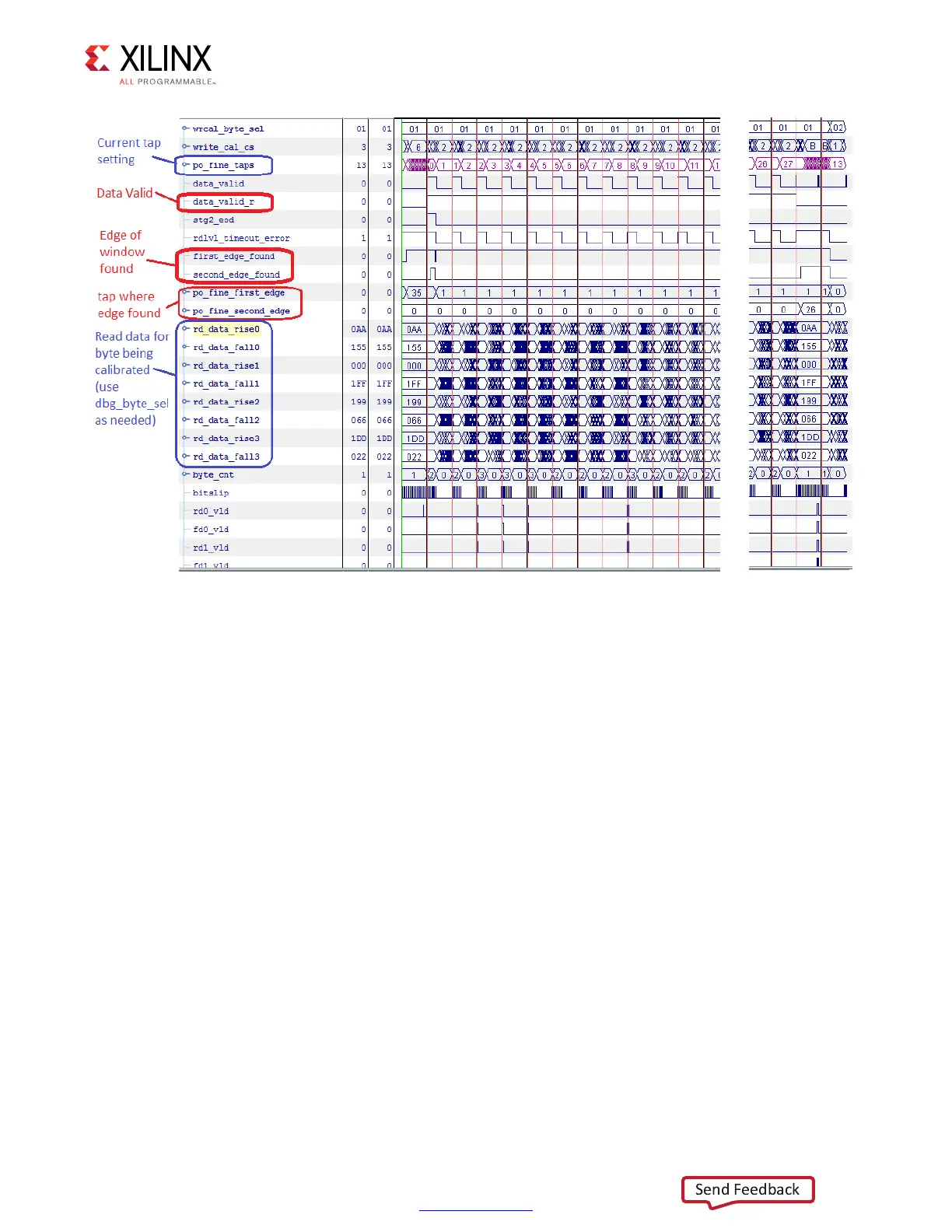
When looking for issues, check to see if the read data being returned for a given byte lane
is correct, as indicated by the data_valid_r signal. This signal checks the data across
multiple clock cycles to ensure all data written during the burst is properly received. If you
see gaps in this signal, this might indicate most of the data was written properly but not all
of it was correct. Check to make sure the latency between the command and the data at the
DRAM is correct for the given settings selected.
Next, check where the algorithm finds the edges of the window and compare with the data
being received. If the data being received is always wrong, this can indicate an issue with
the read leveling performed in an earlier step of calibration or indicate an issue on the PCB
that requires additional debug.
CLOCK_DEDICATED_ROUTE Constraints
System Clock
If the SRCC/MRCC I/O pin and PLL are not allocated in the same bank, the
CLOCK_DEDICATED_ROUTE constraint must be set to BACKBONE. RLDRAM II/RLDRAM 3
manages these constraints for designs generated with the System Clock option selected as
Differential/Single-Ended (at FPGA Options > System Clock).
X-Ref Target - Figure 3-79
Figure 3-79: Vivado Logic Analyzer Feature Capture of Write Calibration
 Loading...


