Zynq-7000 AP SoC and 7 Series FPGAs MIS v4.1 395
UG586 November 30, 2016
www.xilinx.com
Chapter 3: RLDRAM II and RLDRAM 3 Memory Interface Solutions
FPGA Options
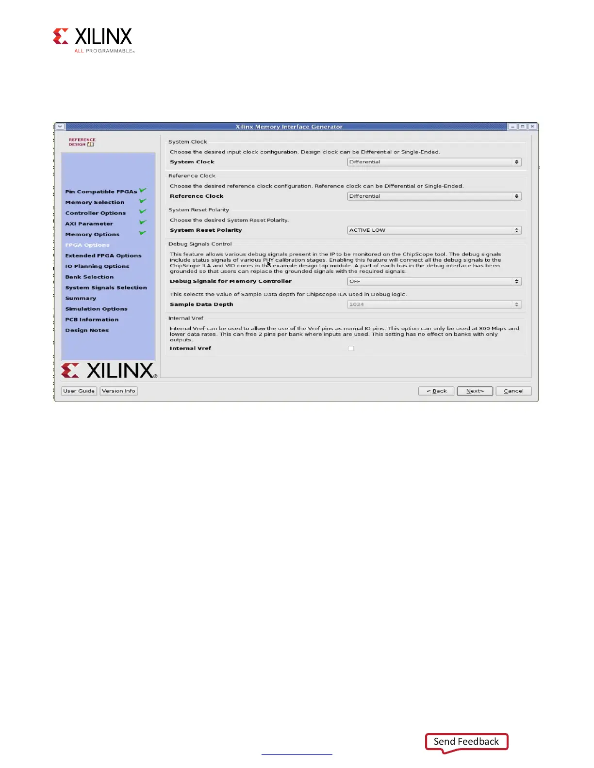
Figure 3-20 shows the FPGA Options page.
• System Clock – This option selects the clock type (Single-Ended, Differential, or No
Buffer) for the sys_clk signal pair. When the No Buffer option is selected, IBUF
primitives are not instantiated in RTL code and pins are not allocated for the system
clock.
If the designs generated from MIG for the No Buffer option are implemented without
performing changes, designs can fail in implementation due to IBUFs not instantiated
for the sys_clk_i signal. So for No Buffer scenarios, sys_clk_i signal needs to be
connected to an internal clock.
• Reference Clock – This option selects the clock type (Single-Ended, Differential, No
Buffer, or Use System Clock) for the clk_ref signal pair. The Use System Clock option
appears when the input frequency is between 199 and 201 MHz (that is, the Input Clock
Period is between 5,025 ps (199 MHz) and 4,975 ps (201 MHz). When the No Buffer
option is selected, IBUF primitives are not instantiated in RTL code and pins are not
allocated for the reference clock.
X-Ref Target - Figure 3-20
Figure 3-20: FPGA Options Page
 Loading...


