Zynq-7000 AP SoC and 7 Series FPGAs MIS v4.1 584
UG586 November 30, 2016
www.xilinx.com
Chapter 4: LPDDR2 SDRAM Memory Interface Solution
rd_data
This bus is the data that was read from the external memory. It can be connected to the data
input of a buffer in the user design.
rd_data_addr
This bus is an echo of data_buf_addr when the current read request is submitted. This
bus can be combined with the rd_data_offset signal and applied to the address input of
a buffer in the user design.
rd_data_en
This signal indicates when valid read data is available on rd_data for a read request. It can
be tied to the chip select and write enable of a buffer in the user design.
rd_data_offset
This bus is used to step through the data buffer when the burst length requires more than
a single cycle to complete. This bus can be combined with rd_data_addr and applied to
the address input of a buffer in the user design.
Native Interface Maintenance Command Signals
Table 4-20 lists the native interface maintenance command signals.
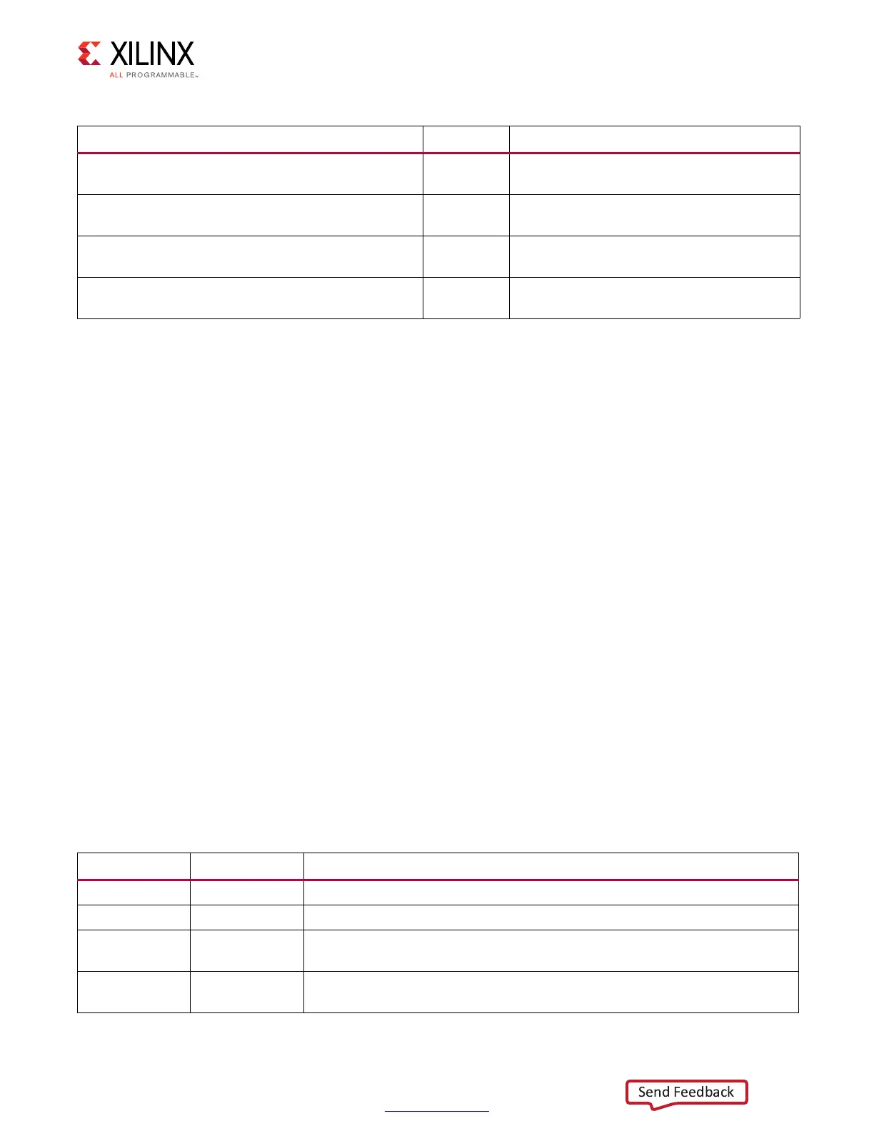
Table 4-19: Native Interface Read Command Signals
Signal Direction Description
rd_data[2 × nCK_PER_CLK × PAYLOAD_WIDTH – 1:0] Output
This is the output data from read
commands.
rd_data_addr[DATA_BUF_ADDR_WIDTH – 1:0] Output
This output provides the base address of the
destination buffer for read commands.
rd_data_en Output
This output indicates that valid read data is
available on the rd_data bus.
rd_data_offset[1:0] Output
This output provides the offset for the
destination buffer for read commands.
Table 4-20: Native Interface Maintenance Command Signals
Signal Direction Description
app_sr_req Input This input is reserved and should be tied to 0.
app_sr_active Output This output is reserved.
app_ref_req Input
This active-High input requests that a refresh command be issued to the
DRAM.
app_ref_ack Output
This active-High output indicates that the Memory Controller has sent the
requested refresh command to the PHY interface.
 Loading...


