Zynq-7000 AP SoC and 7 Series FPGAs MIS v4.1 473
UG586 November 30, 2016
www.xilinx.com
Chapter 3: RLDRAM II and RLDRAM 3 Memory Interface Solutions
• Write Data clock (DK_P/N) does not require an external termination, as On-Die
Termination is sufficient.
• Input Clock (CK_P/N) should be differentially terminated with an 80Ω resistor.
• Read Data clock (QK_P/N) does not require an external termination and should use DCI.
Set DCI termination to 40Ω for operation at and above 1,333 Mb/s, or 50Ω if operating
below 1,333 Mb/s.
Manual Pinout Changes
For manually manipulating the parameters described in Table 3-15, the following examples
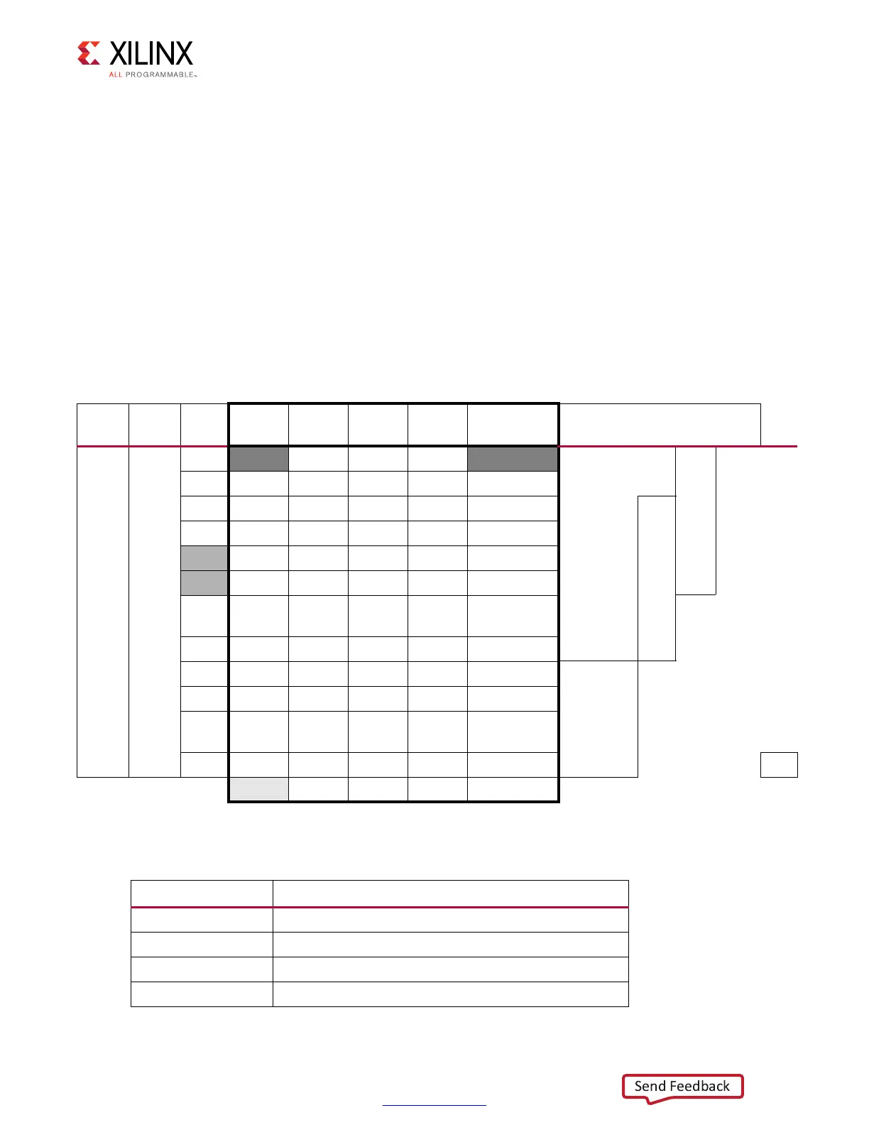
show how to allocate parameters for a given byte lane. Table 3-16 shows a typical RLDRAM
II data byte lane, indicating the bank, byte lane, and bit position for each signal.
The byte lane parameters for Table 3-16 are shown in Table 3-17.
Table 3-16: Example RLDRAM II Byte Lane #1
Bank
Byte
Lane
Bit DDR
Byte
Group
I/O
Type
I/O
Number
Special
Designation
BITLANES
00
9
VREF A_11 P 12 VREF 0
8 DQ8 A_10 N 11 1
7DQ7A_09 P 10 1
6DQ6A_08 N 9 1
B DK0_P A_07 P 8 DQS-P 0 0001
ADK0_NA_06 N 7 DQS-N 0 1
5DQ5A_05 P 6 1
111
1
4DQ4A_04 N 5 1F
3DQ3A_03 P 4 1
2DQ2A_02 N 3 1
1DQ1A_01 P 2 1
111
1
0DQ0A_00 N 1 1 F1FF
VRN N/A SE 0
Table 3-17: Parameters for Example RLDRAM II Data Byte Lane #1
Parameter Value
DK_MAP 8'h00
DQTS_MAP 12'h00A
PHY_0_BITLANES 12'h1FF
DATA0_MAP 108'h008_007_006_005_004_003_002_001_000
 Loading...


