Zynq-7000 AP SoC and 7 Series FPGAs MIS v4.1 116
UG586 November 30, 2016
www.xilinx.com
Chapter 1: DDR3 and DDR2 SDRAM Memory Interface Solution
receives read data from the external memory. The core echoes this address back when the
requests are processed.
Write Command Signals
The native interface has signals that are used when the Memory Controller is processing a
write command (Table 1-52). These signals connect to the control, address, and data signals
of a buffer in the user design.
wr_data
This bus is the data that needs to be written to the external memory. This bus can be
connected to the data output of a buffer in the user design.
wr_data_addr
This bus is an echo of data_buf_addr when the current write request is submitted. The
wr_data_addr bus can be combined with the wr_data_offset signal and applied to
the address input of a buffer in the user design.
wr_data_mask
This bus is the byte enable (data mask) for the data currently being written to the external
memory. The byte to the memory is written when the corresponding wr_data_mask signal
is deasserted.
wr_data_en
When asserted, this signal indicates that the core is reading data from the user design for a
write command. This signal can be tied to the chip select of a buffer in the user design.
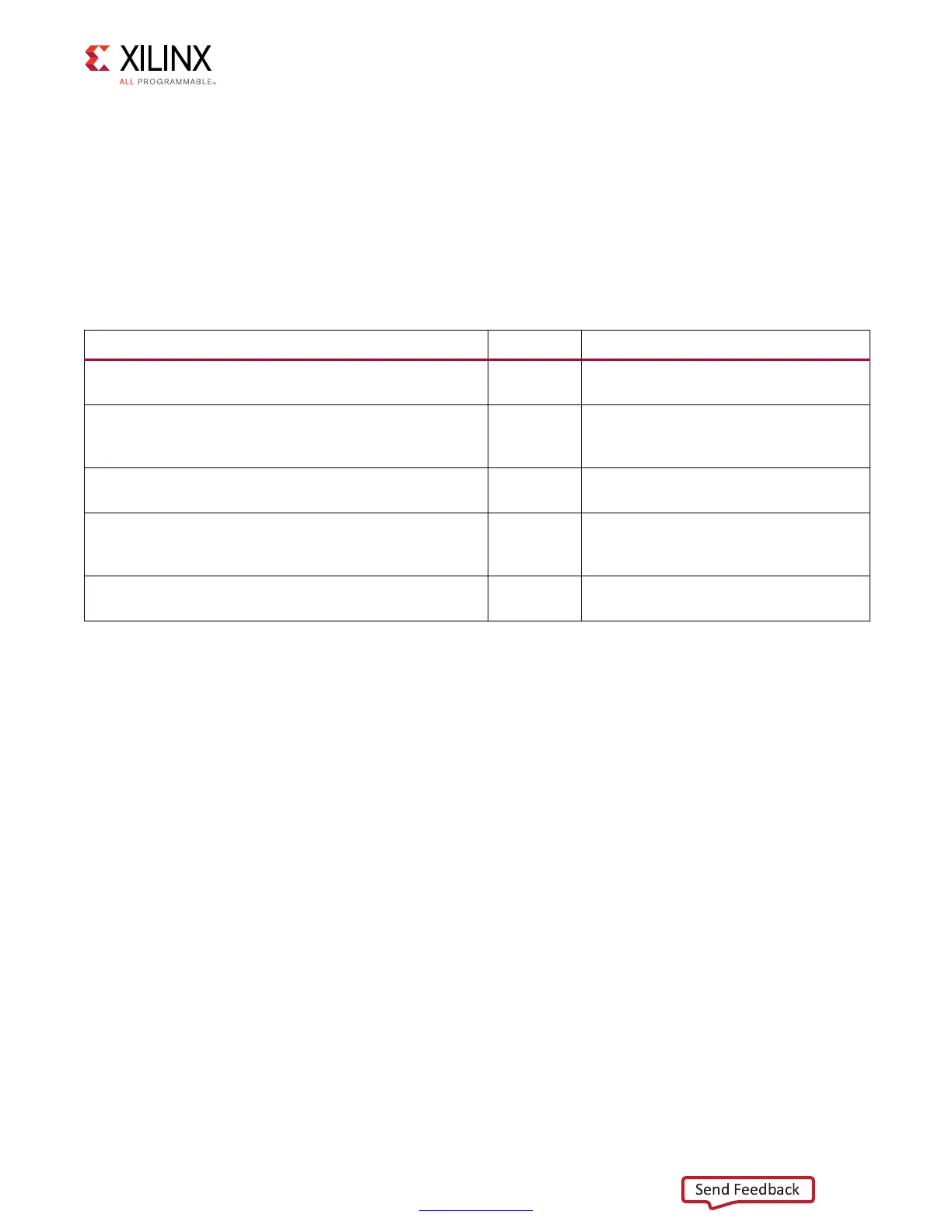
Table 1-52: Native Interface Write Command Signals
Signal Direction Description
wr_data[2 × nCK_PER_CLK × PAYLOAD_WIDTH – 1:0] Input
This is the input data for write
commands.
wr_data_addr [DATA_BUF_ADDR_WIDTH – 1:0] Output
This output provides the base address
for the source data buffer for write
commands.
wr_data_mask[2 × nCK_PER_CLK × DATA_WIDTH/8 – 1:0] Input
This input provides the byte enable for
the write data.
wr_data_en Output
This output indicates that the memory
interface is reading data from a data
buffer for a write command.
wr_data_offset[0:0] Output
This output provides the offset for the
source data buffer for write commands.
 Loading...


