Zynq-7000 AP SoC and 7 Series FPGAs MIS v4.1 609
UG586 November 30, 2016
www.xilinx.com
Chapter 4: LPDDR2 SDRAM Memory Interface Solution
Memory Controller to PHY Interface
The calibration logic module constructs the PHY control word before sending it to the PHY
control block during calibration. After calibration is complete, the
init_calib_complete signal is asserted and sent to the Memory Controller to indicate
that normal operation can begin. To avoid latency increase, the Memory Controller must
send commands in the format required by the dedicated PHY block. As a result, the address,
command, control, and data buses are multiplexed before being sent to the PHY control
block. These buses are driven by the calibration module during the memory initialization
and calibration stages and by the Memory Controller during normal operation. Table 4-24
describes the Memory Controller to PHY interface signals. These signals are synchronous to
the FPGA logic clock.
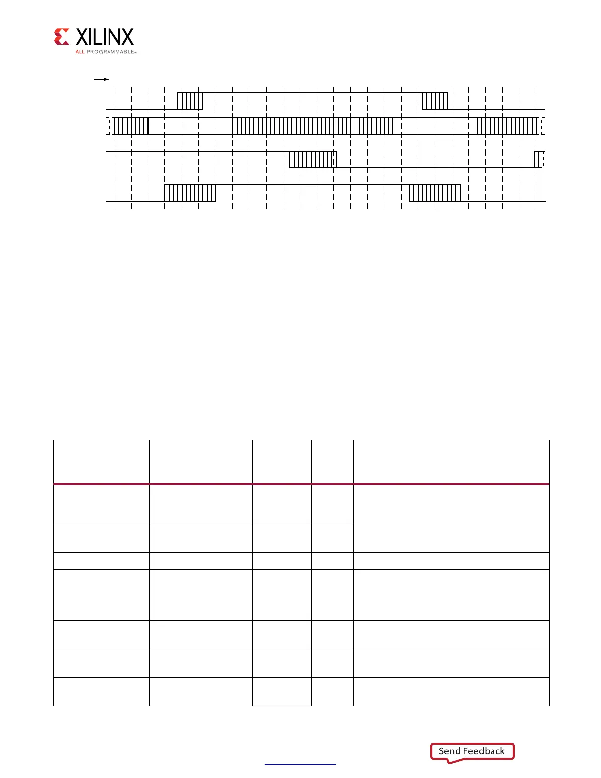
X-Ref Target - Figure 4-55
Figure 4-55: Phase Detector Timing Diagram
4APS
CLK?CPT
5NADJUSTED
EARLY?DQS
!DJUSTED
EARLY?DQS
$1"YTE
!GGREGATE
Table 4-24: Memory Controller to Calibration Logic Interface Signals
Signal Name Width
I/O
To/From
PHY
Type Description
rst 1 Input –
The rstdiv0 output from the infrastructure
module synchronized to the PHY_Clk
domain.
PHY_Clk 1 Input –
This clock signal is 1/4 the frequency of the
LPDDR2 clock.
mem_refclk 1 Input – This is the LPDDR2 frequency clock.
freq_refclk 1 Input –
This signal is the same frequency as
mem_refclk between 400 MHz to 933 MHz,
and 1/2 or 1/4 of mem_refclk for
frequencies below 400 MHz.
sync_pulse 1 Input –
This is the synchronization pulse output by
the PLL.
pll_lock 1 Input –
The LOCKED output of the PLL instantiated
in the infrastructure module.
mc_ca
[CA_WIDTH × 2 ×
nCK_PER_CLK – 1:0]
Input –
mc_ca[2 × CA_WIDTH – 1:0] is the first
command address in the sequence of four.
 Loading...


