Zynq-7000 AP SoC and 7 Series FPGAs MIS v4.1 612
UG586 November 30, 2016
www.xilinx.com
Chapter 4: LPDDR2 SDRAM Memory Interface Solution
The native interface contains no buffers and returns data as soon as possible, but the return
data might be out of order. The application must reorder the received data internally if the
native interface is used and reordering is enabled. The following sections describe timing
protocols of each interface and how they should be controlled.
User Interface
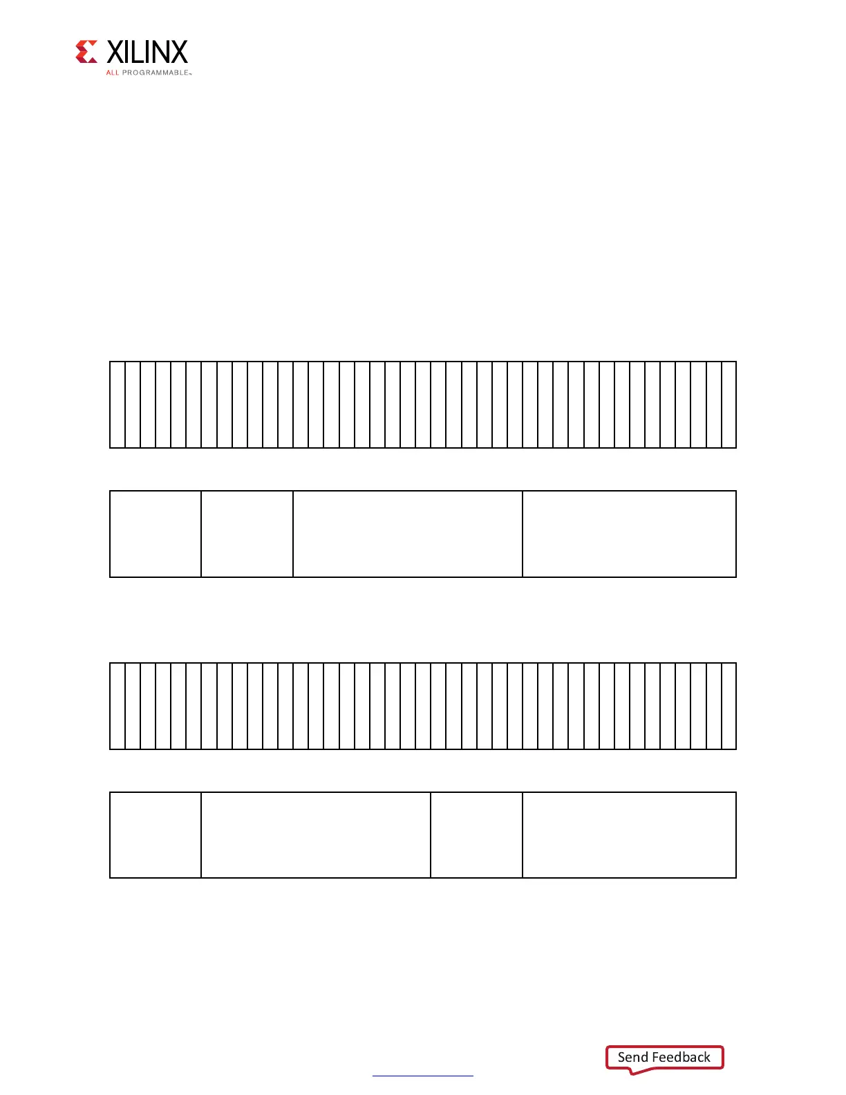
The mapping between the User Interface address bus and the physical memory row, bank
and column can be configured. Depending on how the application data is organized,
addressing scheme Bank- Row-Column or Row-Bank-Column can be chosen to optimize
controller efficiency. These addressing schemes are shown in Figure 4-56 and Figure 4-57.
X-Ref Target - Figure 4-56
Figure 4-56: Memory Address Mapping for Bank-Row-Column Mode in UI Module
5SER!DDRESS
!
N
!
!
!
!
!
!
-EMORY
2ANK "ANK 2OW #OLUMN
5'?C??
X-Ref Target - Figure 4-57
Figure 4-57: Memory Address Mapping for Row-Bank-Column Mode in UI Module
5SER!DDRESS
!
N
!
!
!
!
!
!
-EMORY
2ANK
2OW "ANK
#OLUMN
5'?C?A?
 Loading...


