Zynq-7000 AP SoC and 7 Series FPGAs MIS v4.1 325
UG586 November 30, 2016
www.xilinx.com
Chapter 2: QDR II+ Memory Interface Solution
Interfacing with the Memory Device
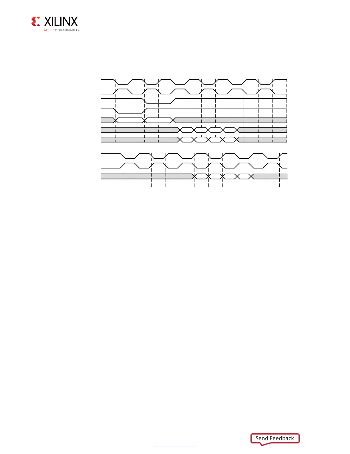
Figure 2-42 shows the physical interface protocol for a four-word memory device.
In four-word burst mode:
• The address is in SDR format
• All signals as input to the memory are center aligned with respect to qdr_k_p
• The data for a write request follows on the next rising edge of qdr_k_p after an
assertion of qdr_w_n
• Byte writes are sampled along with data
•The qdr_q signal is edge aligned to qdr_cq_p and qdr_cq_n
PHY Architecture
The 7 series FPGA PHY is composed of dedicated blocks and soft calibration logic. The
dedicated blocks are structured adjacent to one another with back-to-back interconnects to
minimize the clock and datapath routing necessary to build high-performance physical
layers.
Some of the dedicated blocks that are used in the QDR II+ SRAM PHY and their features are
described as follows:
• I/Os available within each 7 series bank are grouped into four byte groups, where each
byte group consists of up to 12 I/Os.
X-Ref Target - Figure 2-42
Figure 2-42: Four-Word Burst Length Memory Device Protocol
5'?C??
QDR?K?N
QDR?W?N
QDR?R?N
QDR?SA
QDR?D
QDR?BW?N
QDR?Q
QDR?K?P
2$?!$$2 72?!$$2
$7 $7 $7 $7
$7 $7 $7 $7
"7 "7 "7 "7
QDR?CQ?N
QDR?CQ?P
 Loading...


