Zynq-7000 AP SoC and 7 Series FPGAs MIS v4.1 326
UG586 November 30, 2016
www.xilinx.com
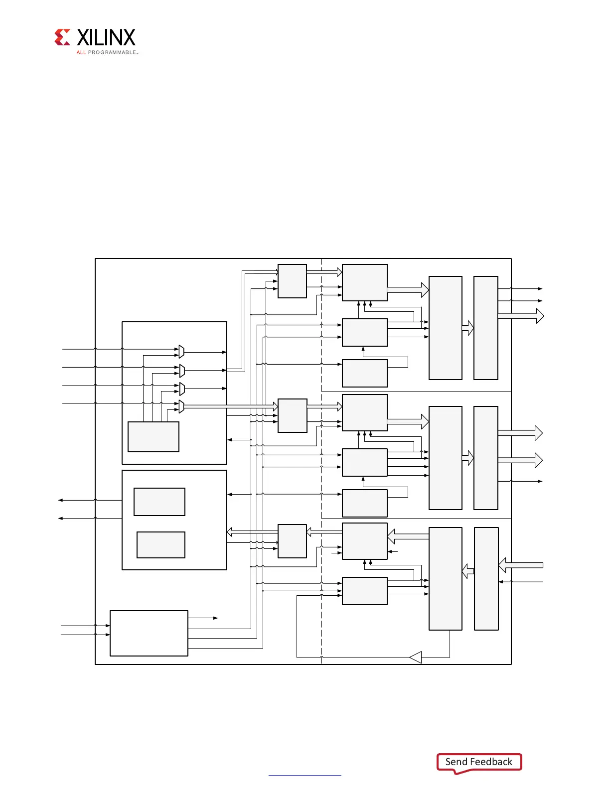
Chapter 2: QDR II+ Memory Interface Solution
• PHASER_IN/PHASER_OUT blocks are available in each byte group and are multi-stage
programmable delay line loops that can provide precision phase adjustment of the
clocks. Dedicated clock within an I/O bank referred to as byte group clocks generated
by the PHASERs help minimize the number of loads driven by the byte group clock
drivers.
• OUT_FIFO and IN_FIFO are shallow 8-deep FIFOs available in each byte group and serve
to transfer data from the FPGA logic domain to the I/O clock domain. OUT_FIFOs are
used to store output data and address/controls that need to sent to the memory while
IN_FIFOs are used to store captured read data before transfer to the FPGA FPGA logic.
The Pinout Requirements section explains the rules that need to be followed while placing
the memory interface signals inside the byte groups.
X-Ref Target - Figure 2-43
Figure 2-43: High-Level PHY Block Diagram for a 36-Bit QDR II+ Interface
)NITIALIZATION
ANDCALIBRATION
COMMAND
SEQUENCER
0HY?WRITE?TOP
5SER?RD?CMD
5SER?WR?CMD
5SER?RD?ADDR
USER?WR?ADDR
5SER?WR?DATA
USER?BW
!DDRESS#ONTROL"ANK
/54?&)&/S
0(!3%2?
/54?0(9
/,/')#
/3%2$%3
2EADLEVELING
STAGE
0HY?READ?TOP
#LOCKAND2ESET
'ENERATIONBLOCK
3YNC?IN
0HY?CLK
-%-?2%&#,+
&2%1?2%&#,+
RD?CMD
WR?CMD
ADDRESS
WRDATABW
-%-2%&#,+
&2%12%&#,+
)/"
0(!3%2?).
-%-2%&#,+
&2%12%&#,+
)/"
3TAGECALIBRATION
ANDDATAVALID
SIGNALGENERATION
5SER?RD?VALID
5SER?RD?DATA
7RITEDATABANK
2EADDATABANK
QDR?R?N
QDR?W?N
QDR?SA
QDR?D;=
QDR?BW;=
QDR?KK
QDR?Q;=
QDR?CQCQ
3YSTEMCLOCK
3YSTEM2ESET
1$2))32!-0(9)NTERFACE
0(!3%2%&#,+
"5&-2
0(9?#.42,?
",/#+
CTLBUS
-%-2%&#,+
2#,+
2%3%4
/54?&)&/S
0(!3%2?
/54?0(9
/,/')#
/3%2$%3
/#,+$)6
/#,+
-%-2%&#,+
&2%12%&#,+
)/"
0(9?#.42,?
",/#+
/,/')#RST
CTLBUS
-%-2%&#,+
2#,+
2%3%4
/#,+$%,!9%$
/#,+$)6
/#,+
/,/')#RST
),/')#
)$%,!9
)3%2$%3
).?&)&/S
)#,+$)6
),/')#RST
7#,+
2%3%4
7#,+
7#,+
2#,+
)#,+
#,+
&2%1""
#1
0/34?&)&/
72%.
2$%.
2$%.
#,+
1
$
1$
02%?&)&/
72%.
#,+
$
1
72%.
$
2$%. 2$%.
72%.
#,+
$
1
!$$2#-$
02%?&)&/
72%.
$
5'?C??
 Loading...


