Zynq-7000 AP SoC and 7 Series FPGAs MIS v4.1 192
UG586 November 30, 2016
www.xilinx.com
Chapter 1: DDR3 and DDR2 SDRAM Memory Interface Solution
Design Guidelines
Guidelines for DDR2 and DDR3 SDRAM designs are covered in this section.
For general PCB routing guidelines, see Appendix A, General Memory Routing Guidelines.
DDR3 SDRAM
This section describes guidelines for DDR3 SDRAM designs, including bank selection, pin
allocation, pin assignments, termination, I/O standards, and trace lengths.
Design Rules
Memory types, memory parts, and data widths are restricted based on the selected FPGA,
FPGA speed grade, and the design frequency. The final frequency ranges are subject to
characterization results.
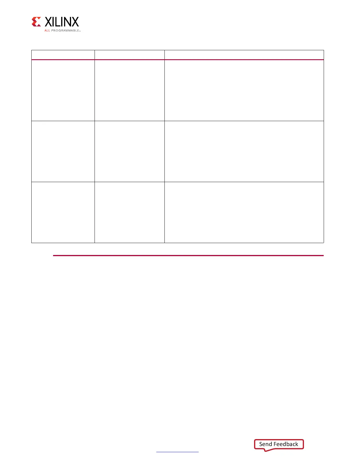
DQS_BYTE_MAP
Bank and byte lane
position information for
the strobe. See the
CK_BYTE_MAP description.
This parameter varies
based on the pinout and
should not be changed
manually in generated
design.
See the CK_BYTE_MAP example.
DATA0_MAP,
DATA1_MAP,
DATA2_MAP,
DATA3_MAP,
DATA4_MAP,
DATA5_MAP,
DATA6_MAP,
DATA7_MAP,
DATA8_MAP
Bank and byte lane
position information for
the data bus. See the
ADDR_MAP description.
This parameter varies
based on the pinout and
should not be changed
manually in generated
design.
See the ADDR_MAP example.
MASK0_MAP,
MASK1_MAP
Bank and byte lane
position information for
the data mask. See the
ADDR_MAP description.
This parameter varies
based on the pinout and
should not be changed
manually in generated
design.
See the ADDR_MAP example.
Table 1-66: DDR2/DDR3 SDRAM Memory Interface Solution Pinout Parameters (Cont’d)
Parameter Description Example
 Loading...


