Zynq-7000 AP SoC and 7 Series FPGAs MIS v4.1 163
UG586 November 30, 2016
www.xilinx.com
Chapter 1: DDR3 and DDR2 SDRAM Memory Interface Solution
Interfacing to the Core
The Memory Controller can be connected using either the AXI4 slave interface, the UI, or
the native interface. The AXI4 slave interface provides an AXI4 memory-mapped compliant
slave ideal for connecting to processor subsystems. The AXI4 slave interface converts its
transactions to pass them over the UI. The UI resembles a simple FIFO interface and always
returns the data in order. The native interface offers higher performance in some situations,
but is more challenging to use.
The native interface contains no buffers and returns data as soon as possible, but the return
data might be out of order. The application must reorder the received data internally if the
native interface is used and reordering is enabled. The following sections describe timing
protocols of each interface and how they should be controlled.
Note:
For a multi-ported memory interface or an interface that is sending requests faster than the
MIG can consume, putting a packet (store and forward) FIFO on the input side of the user logic side
of the crossbar is necessary. This allows it to buffer the requests and grants bursts to come out as
soon as it is ready.
AXI4 Slave Interface
The AXI4 slave interface follows the AXI4 memory-mapped slave protocol specification as
described in the ARM AMBA open specifications. See this specification [Ref 4] for the
signaling details of the AXI4 slave interface.
AXI Addressing
The AXI address from the AXI master is a TRUE byte address. The AXI shim converts the
address from the AXI master to the memory based on AXI SIZE and memory data width. The
LSBs of the AXI byte address are masked to 0, depending on the data width of the memory
array. If the memory array is 64 bits (8 bytes) wide, AXI address[2:0] are ignored and treated
as 0. If the memory array is 16 bits (2 bytes) wide, AXI address[0] is ignored and treated as 0.
DDR3 DRAM is accessed in blocks of eight DRAM words for a burst length of 8. The UI data
port is as wide as eight DRAM words for 4:1 PHY to Memory Controller (MC) clock ratio
mode and four DRAM words for 2:1 PHY to MC clock ratio.
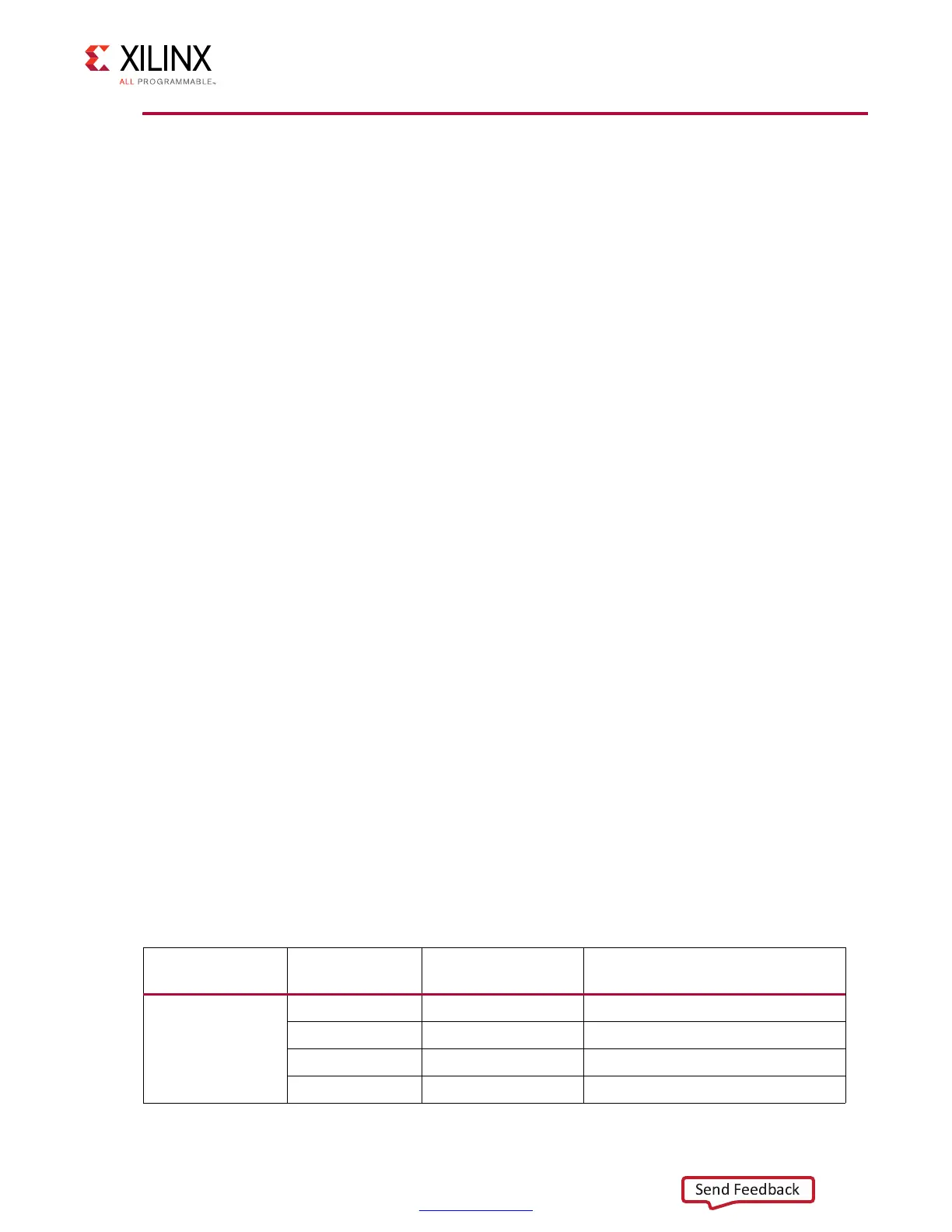
Table 1-62: AXI Byte Address Masking
PHY to MC Clock
Ratio
UI Data Width
Memory Interface
Data Width
AXI Byte Address [7:0] (LSBs)
Masking
4:1
64 8 A[7:0]
128 16 A[7:1], 1’b0
256 32 A[7:2], 2’b00
512 64 A[7:3], 3’b000
 Loading...


