Zynq-7000 AP SoC and 7 Series FPGAs MIS v4.1 506
UG586 November 30, 2016
www.xilinx.com
Chapter 3: RLDRAM II and RLDRAM 3 Memory Interface Solutions
Read Stage 1 Calibration Debug Signals
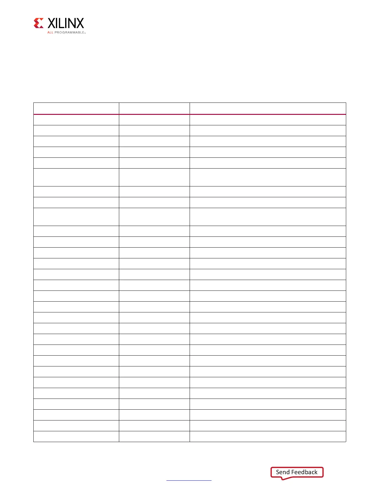
Table 3-30 indicates the mapping between bits within the dbg_rd_stage1_cal bus and
debug signals in the PHY. All signals are found within the qdr_rld_phy_rdlvl module
and are all valid in the clk domain.
Table 3-30: Read Stage 1 Debug Signal Map
Bits PHY Signal Name Description
dbg_rd_stage1_cal[2:0] sm_r Read level main state machine.
dbg_rd_stage1_cal[7:6] seq_sm_r Read level sequence state bits.
dbg_rd_stage1_cal[14:12] rdlvl_work_lane_r Lane currently undergoing read level calibration.
dbg_rd_stage1_cal[15] rdlvl_stg1_start Write side signal causing read level block to start.
dbg_rd_stage1_cal[16] rdlvl_stg1_done Read level block signals completion.
dbg_rd_stage1_cal[17] rdlvl_stg1_start
Write side signal causing read level to copy first lane
result across all lanes.
dbg_rd_stage1_cal[25:18] rdlvl_stg1_cal_bytes_r Lanes for which write side is requesting calibration.
dbg_rd_stage1_cal[31] cmplx_rdcal_start Write side signal causing read level to do complex cal.
dbg_rd_stage1_cal[32] cmplx_rd_data_valid
Write side signal informing read level that complex read
data is valid.
dbg_rd_stage1_cal[48:41] rd_data_comp_r Per byte comparison results for complex calibration.
dbg_rd_stage1_cal[56:49] iserdes_comp_r Per byte comparison results for simple calibration.
dbg_rd_stage1_cal[57] rdlvl_lane_match Overall comparison result for both simple and complex.
dbg_rd_stage1_cal[66:61] largest_left_edge Phaser in taps when the right most left edge was found.
dbg_rd_stage1_cal[72:67] smallest_right_edge Phaser in taps when the left most right edge was found.
dbg_rd_stage1_cal[78:73] mem_out_dec Output of static compensation ROM.
dbg_rd_stage1_cal[81] rdlvl_pi_stg2_f_incdec Controls directing of phaser in stepping.
dbg_rd_stage1_cal[82] rdlvl_pi_en_stg2_f Phaser in step command.
dbg_rd_stage1_cal[85:83] pi_lane_r Lane to which phaser in commands apply.
dbg_rd_stage1_cal[91] prev_match_r Previous sample matched.
dbg_rd_stage1_cal[96:92] match_out_r idelay of last detected invalid to valid match transition.
dbg_rd_stage1_cal[102:97] samp_cnt_r Sample counter.
dbg_rd_stage1_cal[108:103] samps_match_r Cumulative sample match count.
dbg_rd_stage1_cal[109] samp_result_held_r Result from previous sample cycle.
dbg_rd_stage1_cal[154+:40] simp_dlyval_r Five bits per lane dlyval results for simple pattern.
dbg_rd_stage1_cal[194+:48] simp_left_r Six bits per lane left results for simple pattern.
dbg_rd_stage1_cal[194+:48] simp_right_r Six bits per lane right results for simple pattern.
dbg_rd_stage1_cal[194+:48] simp_center_r Six bits per lane center results for simple pattern.
dbg_rd_stage1_cal[378+:48] cmplx_left_r Six bits per lane left results for complex pattern.
dbg_rd_stage1_cal[426+:48] cmplx_right_r Six bits per lane right results for complex pattern.
 Loading...


