Zynq-7000 AP SoC and 7 Series FPGAs MIS v4.1 513
UG586 November 30, 2016
www.xilinx.com
Chapter 3: RLDRAM II and RLDRAM 3 Memory Interface Solutions
Debugging Write Calibration
Due to the length of time required for completing write calibration for
RLDRAM II/RLDRAM 3, it is useful to use the N-sample feature of the Vivado logic analyzer
feature to selectively trigger and display a small window after a given trigger point. This
allows you to capture signals across a larger period of time than would be allowed if you
just captured a single window when the trigger condition first occurs. A good trigger
condition is the wrcal_byte_sel signal as well as the state machine indicator,
write_cal_cs (see Table 3-32).
This allows you to focus in on a given byte lane and capture each time an adjustment is
made to the PHASER_OUT. An example of what to look for is shown in Figure 3-79.
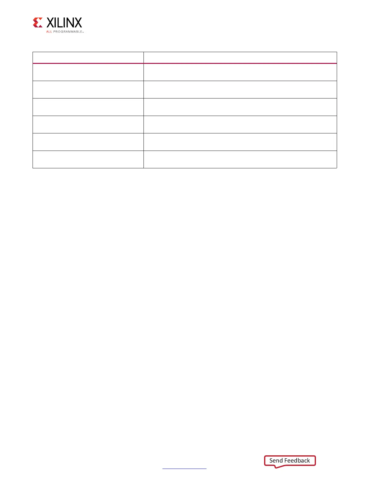
dbg_win_current_bit[6:0]
Feedback to indicate which bit is currently being monitored during
automatic window checking.
dbg_win_current_byte[3:0]
Feedback to indicate which byte is currently being monitored (and
used to select the byte lane controls with dbg_byte_sel).
dbg_win_left_ram_out [WIN_SIZE – 1:0]
PHASER_IN tap count to reach the left edge of the read window for a
given bit.
dbg_win_right_ram_out [WIN_SIZE –
1:0]
PHASER_IN tap count to reach the right edge of the read window for a
given bit.
dbg_pi_f_inc
chk_win control signal to increment PHASER_IN. This signal should be
used only when dbg_win_active is deasserted.
dbg_pi_f_dec
chk_win control signal to decrease PHASER_IN. This signal should be
used only when dbg_win_active is deasserted.
Table 3-33: Debug Port Signals (Cont’d)
Signal Description
 Loading...


