Zynq-7000 AP SoC and 7 Series FPGAs MIS v4.1 393
UG586 November 30, 2016
www.xilinx.com
Chapter 3: RLDRAM II and RLDRAM 3 Memory Interface Solutions
• Data Width – The data width value can be selected here based on the memory part
selected. The MIG tool supports values in multiples of the individual device data widths.
• Data Mask – This option allocates data mask pins when selected. This option should be
deselected to deallocate data mask pins and increase pin efficiency.
• Memory Details – The bottom of the Controller Options page. Figure 3-18 displays
the details for the selected memory configuration.
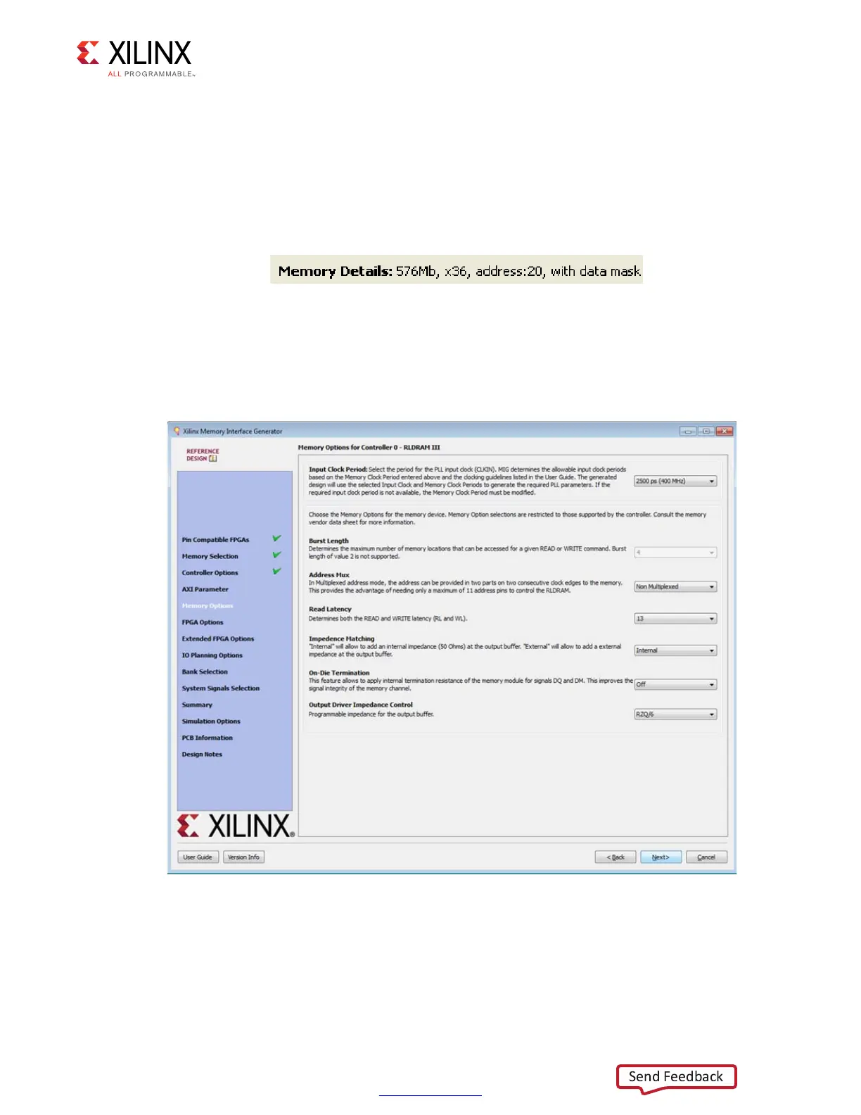
Memory Options
This feature allows the selection of various memory mode register values, as supported by
the controller specification (Figure 3-19).
X-Ref Target - Figure 3-18
Figure 3-18: Selected Memory Configuration Details
X-Ref Target - Figure 3-19
Figure 3-19: Memory Options Page
 Loading...


