EasyManuals Logo

Xilinx Zynq-7000 User Manual

Xilinx Zynq-7000
678 pages
To Next Page IconTo Next Page
To Previous Page IconTo Previous Page
Page #496 background imageLoading...
Page #496 background image
Zynq-7000 AP SoC and 7 Series FPGAs MIS v4.1 496
UG586 November 30, 2016
www.xilinx.com
Chapter 3: RLDRAM II and RLDRAM 3 Memory Interface Solutions
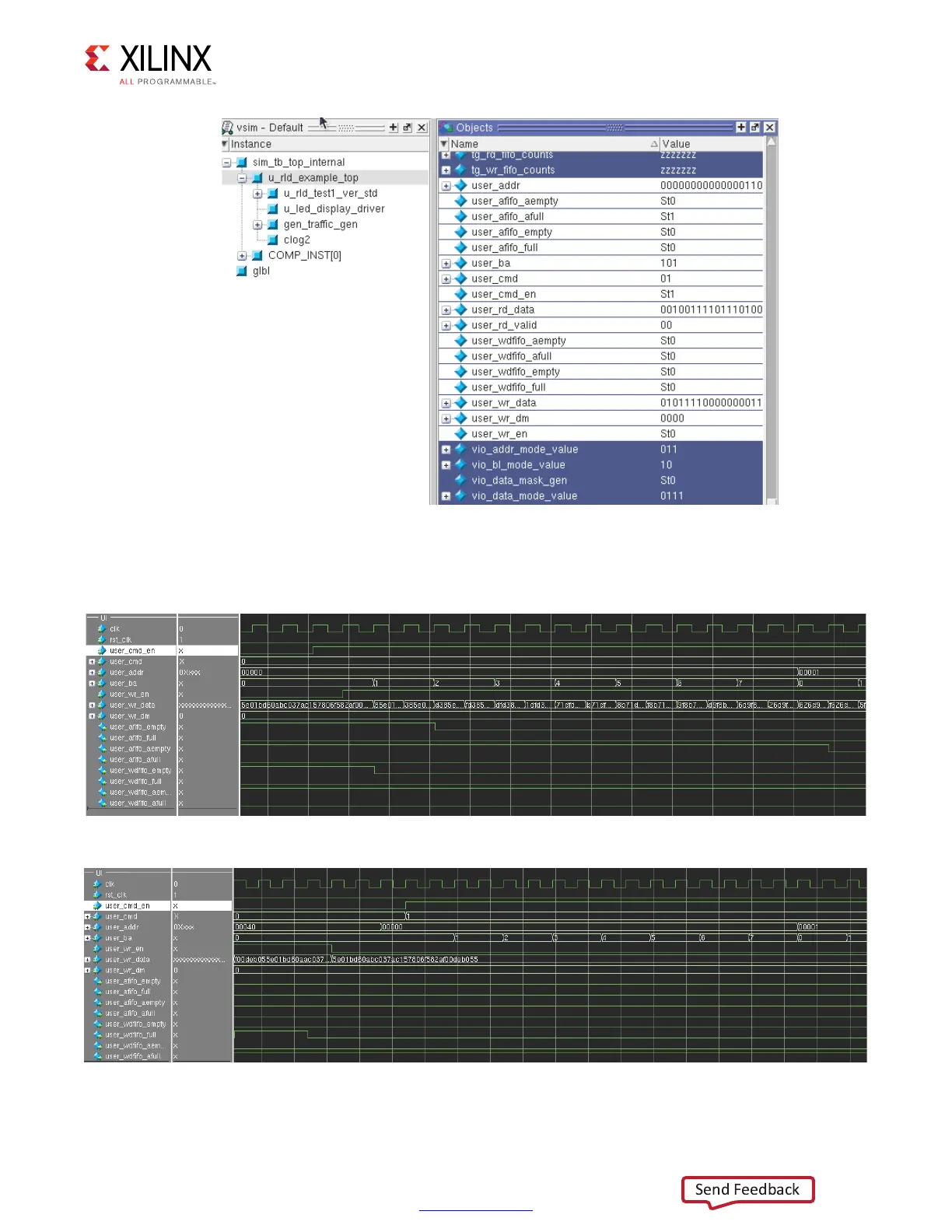
Figure 3-75 and Figure 3-76 show example waveforms of a write and read on both the user
interface.
X-Ref Target - Figure 3-74
Figure 3-74: Questa Advanced Simulator Instance Window
X-Ref Target - Figure 3-75
Figure 3-75: User Interface Write
X-Ref Target - Figure 3-76
Figure 3-76: User Interface Read
Send Feedback

Table of Contents

Other manuals for Xilinx Zynq-7000

Questions and Answers:

Question and Answer IconNeed help?

Do you have a question about the Xilinx Zynq-7000 and is the answer not in the manual?

Xilinx Zynq-7000 Specifications

General IconGeneral
SeriesZynq-7000
Number of CoresDual-core
Processor SpeedUp to 1 GHz
Device TypeSoC
Logic CellsUp to 350K
DSP SlicesUp to 900
External Memory InterfacesDDR3, DDR2, LPDDR2
I/O StandardsLVCMOS, HSTL, SSTL
Operating Temperature-40°C to +100°C (Industrial), 0°C to +85°C (Commercial)
Package OptionsVarious BGA packages
I/O Voltage3.3V

Related product manuals