Zynq-7000 AP SoC and 7 Series FPGAs MIS v4.1 593
UG586 November 30, 2016
www.xilinx.com
Chapter 4: LPDDR2 SDRAM Memory Interface Solution
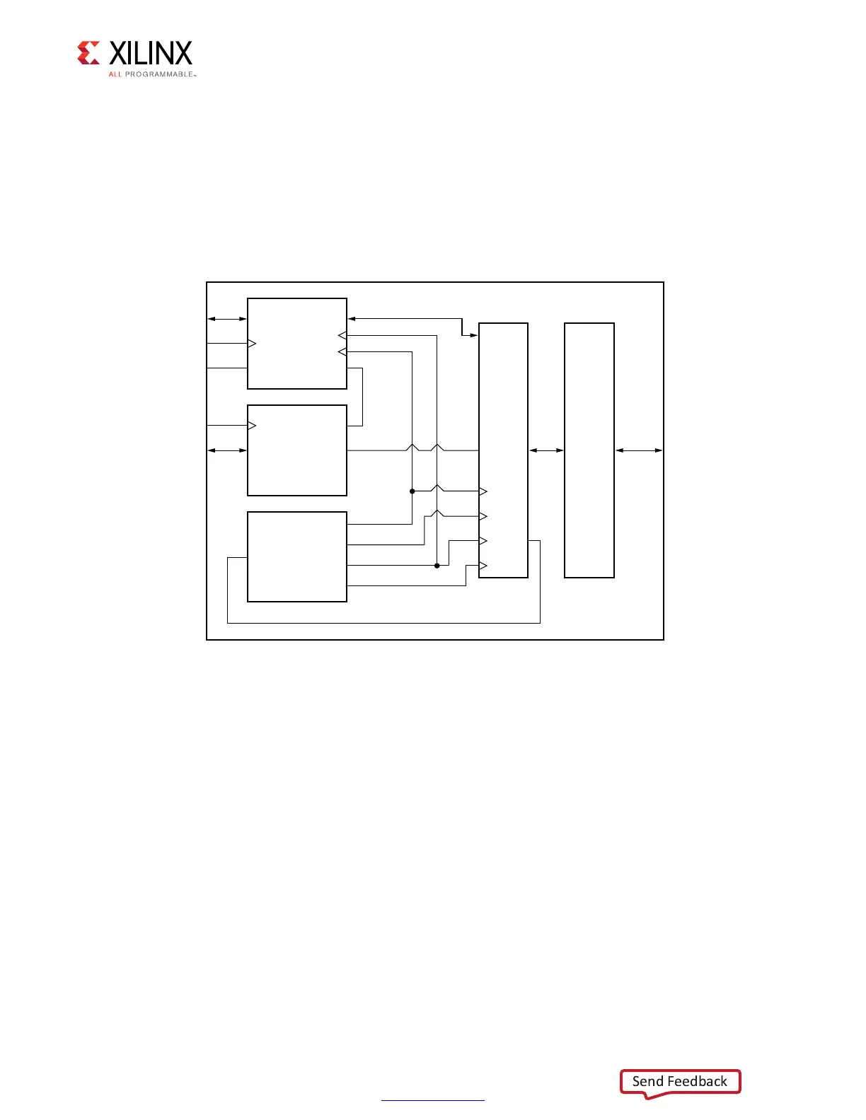
Each 7 series FPGA I/O bank has dedicated blocks comprising a PHY control block, four
PHASER_IN and PHASER_OUT blocks, four IN/OUT_FIFOs, IOLOGIC (ISERDES, OSERDES,
ODDR, IDELAY), and IOBs. Four byte groups exist in an I/O bank, and each byte group
contains the PHASER_IN and PHASER_OUT, IN_FIFO and OUT_FIFO, and twelve IOLOGIC and
IOB blocks. Ten of the twelve IOIs in a byte group are used for DQ and DM bits, and the
other two IOIs are used to implement differential DQS signals. Figure 4-47 shows the
dedicated blocks available in a single I/O bank. A single PHY control block communicates
with all four PHASER_IN and PHASER_OUT blocks within the I/O bank.
The Memory Controller and calibration logic communicate with this dedicated PHY in the
slow frequency clock domain, which is either a divided by 4 or divided by 2 version of the
LPDDR2 memory clock. A block diagram of the PHY design is shown in Figure 4-48.
X-Ref Target - Figure 4-47
Figure 4-47: Single Bank LPDDR2 PHY Block Diagram
)/
&)&/S
0(9
#ONTROL
)/,/')#
)/"
#+#+#+%
#3$$2?#!;=
$ATA;=
$13;=
$13;=
)/0HASERS
$13
/UT"#LK
/UT$"#LK
)N"#LK
)N$"#LK
0HY?!DDR
0HY?#MD
0HY?$ATA
0HY?2D7R?%N
0HY?#LK
#ONTROL
7ORD%NABLES3TATUS
0HY?#LK
 Loading...


