Zynq-7000 AP SoC and 7 Series FPGAs MIS v4.1 433
UG586 November 30, 2016
www.xilinx.com
Chapter 3: RLDRAM II and RLDRAM 3 Memory Interface Solutions
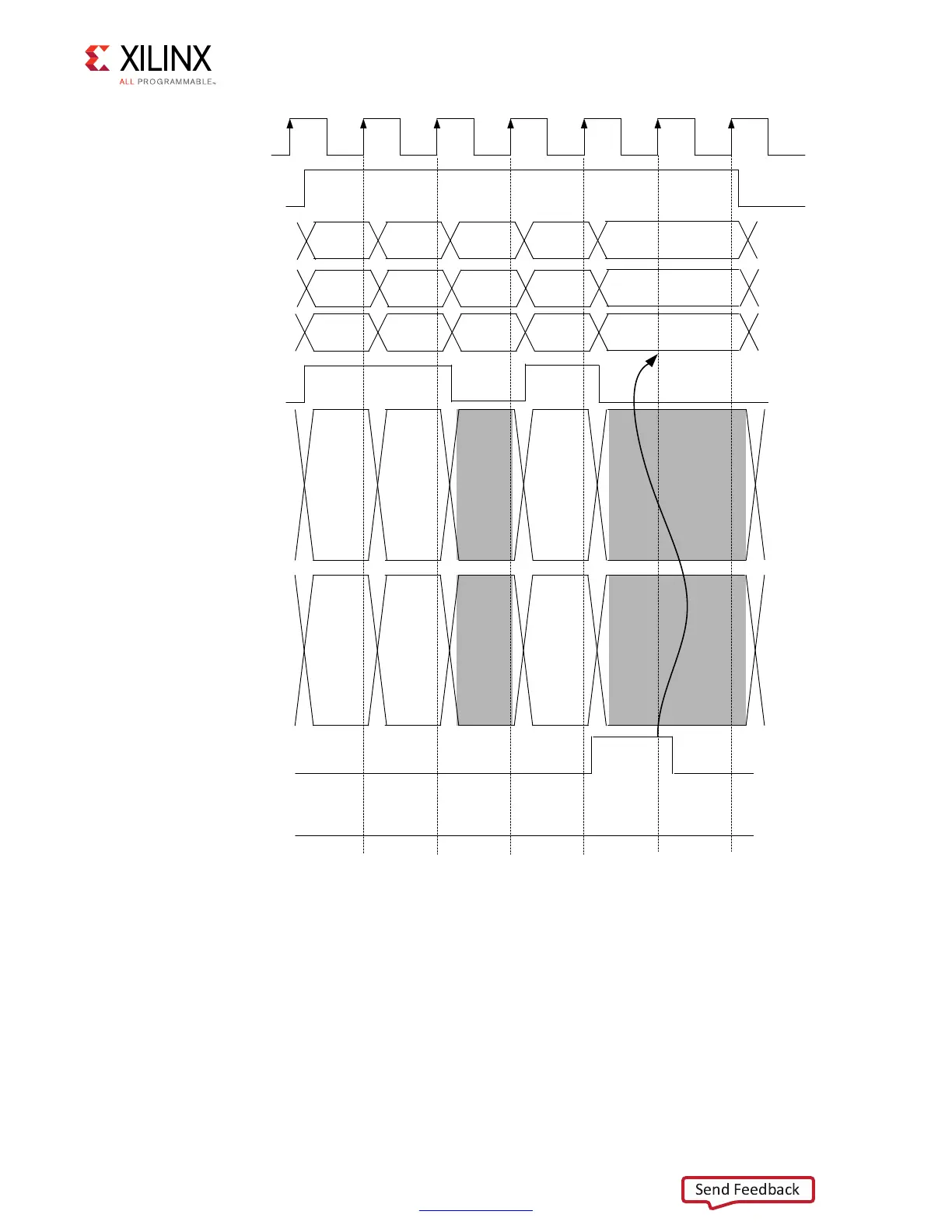
When a read command is issued some time later (based on the configuration and latency of
the system), the user_rd_valid[0] signal is asserted, indicating that user_rd_data is
now valid, while user_rd_valid[1] is asserted indicating that user_rd_data is valid,
as shown in Figure 3-44. The read data should be sampled on the same cycle that
user_rd_valid[0] and user_rd_valid[1] are asserted because the core does not
buffer returning data. If desired, you can add this functionality.
The Memory Controller only puts commands on certain slots to the PHY such that the
user_rd_valid signals are all asserted together and return the full width of data, but the
extra user_rd_valid signals are provided in case of controller modifications.
X-Ref Target - Figure 3-43
Figure 3-43: RLDRAM 3 Client Interface Protocol (Eight-Word Burst Architecture)
#,+
USER?CMD?EN
!
USER?ADDR
USER?WR?EN
!
"! "!
USER?BA
USER?WR?DATA
USER?CMD
! !
"! "!
USER?WR?DM
WRITEWRITE READ
WRITE
USER?AFIFO?FULL
USER?WDFIFO?FULL
!
"!
READ
READ
!
"!
8
[FALL
RISE
FALL
RISE
FALL
RISE
FALL
RISE]
[FALL
RISE
FALL
RISE
FALL
RISE
FALL
RISE]
[FALL
RISE
FALL
RISE
FALL
RISE
FALL
RISE]
[FALL
RISE
FALL
RISE
FALL
RISE
FALL
RISE]
[FALL
RISE
FALL
RISE
FALL
RISE
FALL
RISE]
[FALL
RISE
FALL
RISE
FALL
RISE
FALL
RISE]
 Loading...


