Zynq-7000 AP SoC and 7 Series FPGAs MIS v4.1 169
UG586 November 30, 2016
www.xilinx.com
Chapter 1: DDR3 and DDR2 SDRAM Memory Interface Solution
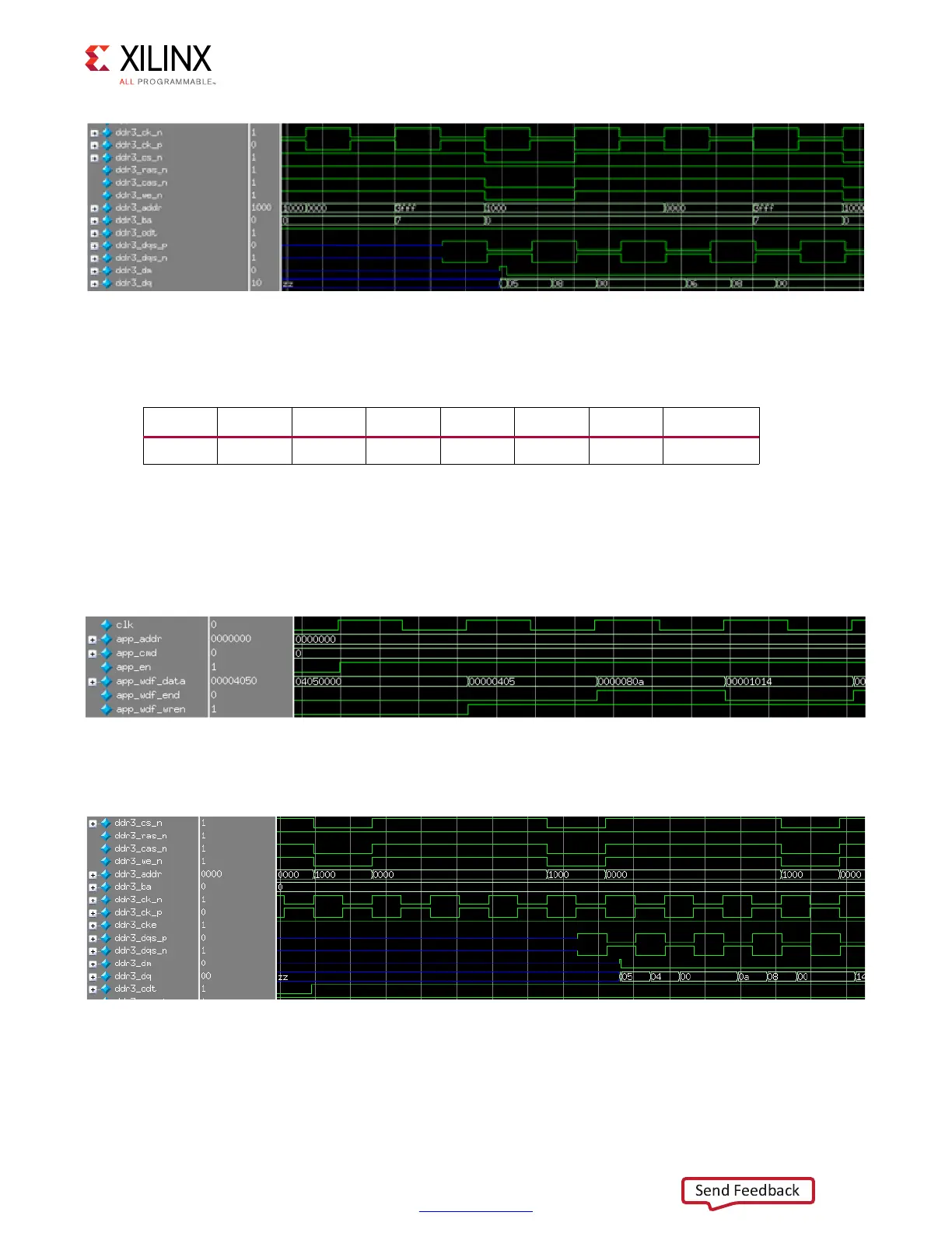
The data values at different clock edges are as shown in Table 1-63.
For a 2:1 Memory Controller to DRAM clock ratio, the application data width is 32 bits.
Hence for BL8 transactions, the data at the application interface must be provided in two
clock cycles. The app_wdf_end signal is asserted for the second data as shown in
Figure 1-79. In this case, the application data provided in the first cycle is 0000_0405 (Hex),
and the data provided in the last cycle is 0000_080A (Hex). This is for a BL8 transaction.
Figure 1-80 shows the corresponding data at the DRAM interface.
X-Ref Target - Figure 1-78
Figure 1-78: Data at the DRAM Interface for 4:1 Mode
Table 1-63: Data Values at Different Clock Edges
Rise0 Fall0 Rise1 Fall1 Rise2 Fall2 Rise3 Fall3
05 08 00 00 06 08 00 00
X-Ref Target - Figure 1-79
Figure 1-79: Data at the Application Interface for 2:1 Mode
X-Ref Target - Figure 1-80
Figure 1-80: Data at the DRAM Interface for 2:1 Mode
 Loading...


