Zynq-7000 AP SoC and 7 Series FPGAs MIS v4.1 603
UG586 November 30, 2016
www.xilinx.com
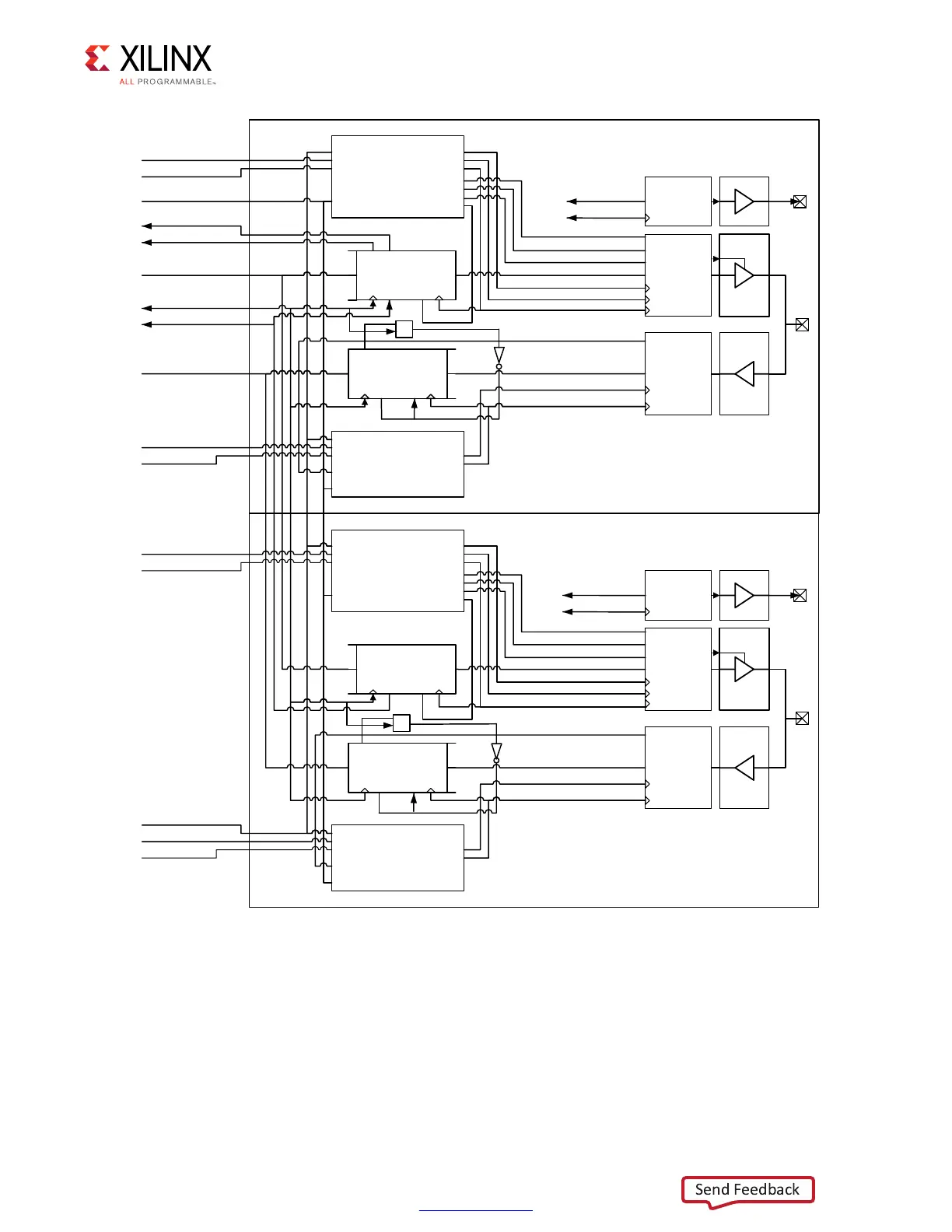
Chapter 4: LPDDR2 SDRAM Memory Interface Solution
Each IN/OUT_FIFO has a storage array of memory elements arranged as 10 groups
eight bits wide and eight entries deep. During a write, the OUT_FIFO receives four bits of
data for each DQ bit from the calibration logic or Memory Controller and writes the data
into the storage array in the PHY_Clk clock domain, which is 1/2 the frequency of the
LPDDR2 SDRAM clock.
X-Ref Target - Figure 4-52
Figure 4-52: Datapath Block Diagram
Out_FIFO_D
D
WEn
REn
Q
WClk
RClk
Full
AF
AE
Empty
In_FIFO_D
DQ
WClk
WEn
REn
RClk
Full
AF
AE
Empty
D_Out[15:8], DM1
D_In[15:8]
WrBClk_D
WrDivBClk_D
RdBClk_D
RdDivBClk_D
PHY_Clk
PHY_WrEn
IBUF
OBUF
WrBClk_90_D
ISERDES
Byte Group
DQS_In_1
DQTriState_D
OSERDES
Byte Group
DQSTriState_D
OF_RE_D
IF_WE_D
tied to 1
PHY_DM[1:0],
PHY_D_Out[15:0]
PHY_D_In[15:0]
Phaser
Out D
OClk1x
OClk1x90
OClkDiv
PhaseRef
FreqRef
CTS[1:0]
DTS[1:0]
RdEnable
DQS[1:0]
RankSel[1:0]
Enable_Calib[1:0]
Burst_Pending
Phaser
In D
IClk1x
IClkDiv
PhaseRef
FreqRef
Enable_Calib[1:0]
Burst_Pending
RankSel[1:0]
RClk
WriteEnable
PHY_OF_Full
PHY_OF_AlmostFull
DQS_D
Out_FIFO_C
D
WEn
REn
Q
WClk
RClk
Full
AF
AE
Empty
In_FIFO_C
DQ
WClk
WEn
REn
RClk
Full
AF
AE
Empty
D_Out[7:0], DM0
WrBClk_C
WrDivBClk_C
RdBClk_C
RdDivBClk_C
IBUF
OBUF
WrBClk_90_C
ISERDES
Byte Group
DQS_In_0
DQTriState_C
OSERDES
Byte Group
DQSTriState_C
OF_RE_C
Phaser
Out C
OClk1x
OClk1x90
OClkDiv
PhaseRef
FreqRef
CTS[1:0]
DTS[1:0]
RdEnable
DQS[1:0]
RankSel[1:0]
Enable_Calib[1:0]
Burst_Pending
Phaser
In C
IClk1x
IClkDiv
PhaseRef
FreqRef
Enable_Calib[1:0]
Burst_Pending
RankSel[1:0]
RClk
WriteEnable
DQS_C
D_In[7:0]
Out_Rank_D[1:0]
Out_Burst_Pending[3]
In_Rank_D[1:0]
In_Burst_Pending[3]
In_Rank_C[1:0]
In_Burst_Pending[2]
PC_Enable_Calib[1:0]
Out_Rank_C[1:0]
Out_Burst_Pending[2]
Freq_Ref_Clk
Data Byte Group D
Data Byte Group C
OFF
Note: RESET_N is implemented as a
SDR OFF clocked by DDR_Clk
OBUF
DDR_RESET_N
DDR_DivR_Clk
Note: CKE is implemented as a SDR
OFF clocked by DDR_Clk
OBUF
DDR_CKE
DDR_DivR_Clk
OFF
1'b1
IF_WE_C
tied to 1
1'b1
 Loading...


