EasyManua.ls Logo

Analog Devices ADuCM356 User Manual

Analog Devices ADuCM356
312 pages
To Next Page IconTo Next Page
To Previous Page IconTo Previous Page
Page #104 background imageLoading...
Page #104 background image
Reference Manual ADuCM356
HIGH-SPEED DAC CIRCUITS
analog.com Rev. A | 104 of 312
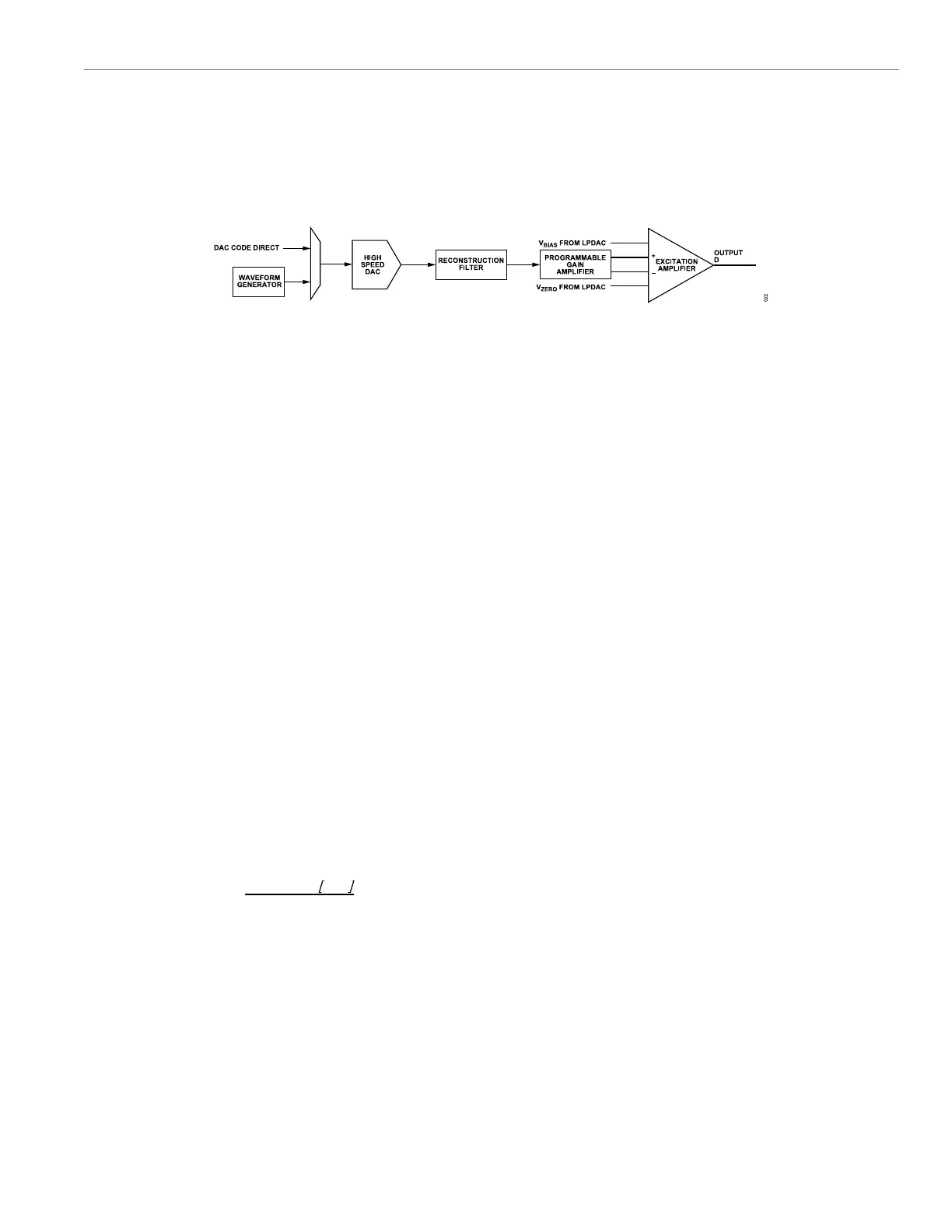
The 12-bit high-speed DAC generates an AC excitation signal
when measuring the impedance of an external sensor. The DAC
output signal can be controlled directly by writing to a data register
or by the automated waveform generator block. The high-speed
DAC signal is fed to an excitation amplifier designed specifically to
couple the AC signal on top of the normal DC bias voltage of the
sensor. Alternatively, the high-speed DAC can be used as a normal
voltage source. See the Calibrating the High-Speed DAC section
for more details.
Figure 23. Overview of High-Speed DAC Blocks
HIGH-SPEED DAC OUTPUT SIGNAL
GENERATION
There are two ways of setting the high-speed DAC output voltage,
which are as follows:
â–º Direct write to the DAC code register. Write to the HSDACDAT
register, a 12-bit register where the MSB is a sign bit. A value of
0x800 results in a 0 V output. 0xFFF is positive full scale. 0x000
is negative full scale.
â–º Use the automatic waveform generator. The waveform generator
can be programmed to generate fixed frequency and fixed ampli-
tude signals. If the user selects the sine wave, options exist to
adjust the offset and phase of the output signal.
To use the waveform generator to generate a sine wave, follow
these steps:
1. Set AFECON, Bit 14 = 1 to turn on the waveform generator.
2. Set WGCON, Bits[2:1] = 10 to select sine waveforms.
3. Set WGAMPLITUDE, Bits[10:0] to set up the sine wave ampli-
tude. The sine wave automatically swings above or below the
common-mode voltage. As such, there are only 11 bits required
for the amplitude control.
4. Set WGFCW, Bits[23:0] to set the sine wave output frequency.
For output frequencies higher than 80 kHz, the high-speed
DAC must be configured for high-power mode. See the Power
Mode Configuration Register section for more details. For this
configuration, use the equation
f
OUT
= f
ACLK
×
WGFCWBits
23: 0
2
30
(11)
where:
f
OUT
is the output frequency.
f
ACLK
is the analog clock frequency, 16 MHz.
HIGH-SPEED DAC CORE POWER MODES
The reference source of the high-speed DAC is an internal 1.8 V
precision reference voltage.
There are three basic modes of operation of the high-speed DAC
that trade power consumption and output speed.
Low-Power Mode
When configuring the high-speed DAC for low-power mode, take
note of the following requirements and features:
â–º Clear PMBW, Bit 0 = 0 to minimize current consumption. This
setting is recommended when the high-speed DAC output fre-
quency must be ≤80 kHz.
â–º In low-power mode, the system clock to the DAC and the ADC is
16 MHz.
â–º Ensure that CLKSEL, Bits[1:0] selects a 16 MHz clock source.
For example, an internal high-speed oscillator is selected if
CLKSEL, Bits[1:0] = 00. Ensure that the system clock divide ratio
is 1 (CLKCON0, Bits[5:0] = 0 or 1).
â–º If the internal high-speed oscillator is selected as the system
clock source, ensure that the 16 MHz option is selected. Set
HPOSCCON, Bit 2 = 1.

Table of Contents

Question and Answer IconNeed help?

Do you have a question about the Analog Devices ADuCM356 and is the answer not in the manual?

Analog Devices ADuCM356 Specifications

General IconGeneral
BrandAnalog Devices
ModelADuCM356
CategoryMicrocontrollers
LanguageEnglish

Summary

PREFACE

SCOPE

Provides a detailed description of the functionality and features of the ADuCM356.

CLOCKING ARCHITECTURE

DIGITAL DIE CLOCK FEATURES

Details the clock sources, dividers, and gating for the digital die system clock.

ANALOG DIE CLOCK FEATURES

Details the clock sources, dividers, and gating for the analog die system clock.

POWER MANAGEMENT UNIT

Active Mode

Describes the fully active operating mode where the Arm Cortex-M3 executes from flash and SRAM.

Flexi Mode

Describes the mode where the Arm Cortex-M3 is disabled, allowing peripherals to operate.

Hibernate Mode

Describes the low-power mode where the digital core and most analog blocks are powered down.

SYSTEM RESETS

DIGITAL DIE RESET OPERATION

Explains the reset sources and operation for the digital die, including software resets.

PROGRAMMING, PROTECTION, AND DEBUG

Debug Features

Details the SWD port, flash patch breakpoints, and data watchpoint/trigger units for debugging.

SYSTEM EXCEPTIONS AND PERIPHERAL INTERRUPTS

CORTEX-M3 AND FAULT MANAGEMENT

Describes the system exceptions and fault handling features integrated with the Cortex-M3 processor.

ANALOG DIE CIRCUITRY SUMMARY

ADC, HIGH-SPEED DAC, AND ASSOCIATED AMPLIFIERS OPERATING MODE CONFIGURATION

Configures the operating modes for ADC, High-Speed DAC, and associated amplifiers.

ADC CIRCUIT

ADC CIRCUIT FEATURES

Lists the key features of the ADuCM356's fast multichannel, 16-bit ADC.

LOW-POWER POTENTIOSTAT AMPLIFIERS AND LOW-POWER TIAS

LOW-POWER POTENTIOSTAT AMPLIFIERS

Details the two low-power potentiostat amplifiers for setting external sensor bias voltage.

HIGH-SPEED DAC CIRCUITS

HIGH-SPEED DAC OUTPUT SIGNAL GENERATION

Explains how to generate high-speed DAC output voltage via direct write or waveform generator.

PROGRAMMABLE SWITCHES CONNECTING THE EXTERNAL SENSOR TO THE HIGH-SPEED DAC AND HIGH-SPEED TIA

DX SWITCHES

Selects pins for the high-speed DAC excitation amplifier output, used for impedance measurements.

SEQUENCER

SEQUENCER COMMANDS

Describes the two types of commands: write commands and timer commands (wait, timeout).

SLEEP AND WAKE-UP TIMER

CONFIGURING A DEFINED SEQUENCE ORDER

Defines the order of sequence execution periodically using the SEQORDER register.

USE CASE CONFIGURATIONS

HIBERNATE MODE WHILE MAINTAINING A DC BIAS TO THE SENSOR

Details setup for hibernate mode while maintaining sensor bias voltage.

DMA CONTROLLER

DMA FEATURES

Lists the features of the ADuCM356's dedicated and independent DMA channels.

FLASH CONTROLLER

SUPPORTED COMMANDS

Summarizes the commands supported by the flash controller for read, write, erase, and signature operations.

REGISTER DETAILS: FLASH CACHE CONTROLLER (FLCC)

COMMAND REGISTER

Allows execution of specified flash commands like write, erase, abort, and signature generation.

DIGITAL INPUTS AND OUTPUTS

DIGITAL INPUTS AND OUTPUTS OPERATION

Explains how to configure, read, and write digital input and output pins.

I2C SERIAL INTERFACE

I2C OPERATION

Details the steps required to run the I2C peripheral, including startup and modes.

SERIAL PERIPHERAL INTERFACES

SPI OPERATION

Describes the operation of the SPI interface, including initiator and target modes.

REGISTER SUMMARY: SPI0/SPI1

STATUS REGISTERS

Provides status information for SPI0 and SPI1, including ready, overflow, and error conditions.

REGISTER DETAILS: UART

INTERRUPT ENABLE REGISTER

Configures which interrupt sources generate an interrupt for the UART.

DIGITAL DIE GENERAL-PURPOSE TIMERS

GENERAL-PURPOSE TIMER OPERATIONS

Explains the operation of timers in free running mode and periodic mode.

REGISTER SUMMARY: ANALOG DIE GENERAL-PURPOSE TIMERS

CONTROL REGISTER

Controls timer operation, including clock source, mode, and event selection.

REGISTER DETAILS: DIGITAL DIE WAKE-UP TIMER

STATUS 0 REGISTER

Provides status information for WUT operation, including synchronization and pending writes.

CYCLIC REDUNDANCY CHECK

CRC OPERATING MODES

Details the core access and DMA access modes for CRC calculation.

REGISTER SUMMARY: CRC

CRC CONTROL REGISTER

Controls the CRC peripheral, including enabling, mirroring, and calculation order.

HARDWARE DESIGN CONSIDERATIONS

SERIAL WIRE DEBUG INTERFACE

Describes the SWD interface for debugging and programming, replacing JTAG.