Reference Manual ADuCM356
HARDWARE DESIGN CONSIDERATIONS
analog.com Rev. A | 311 of 312
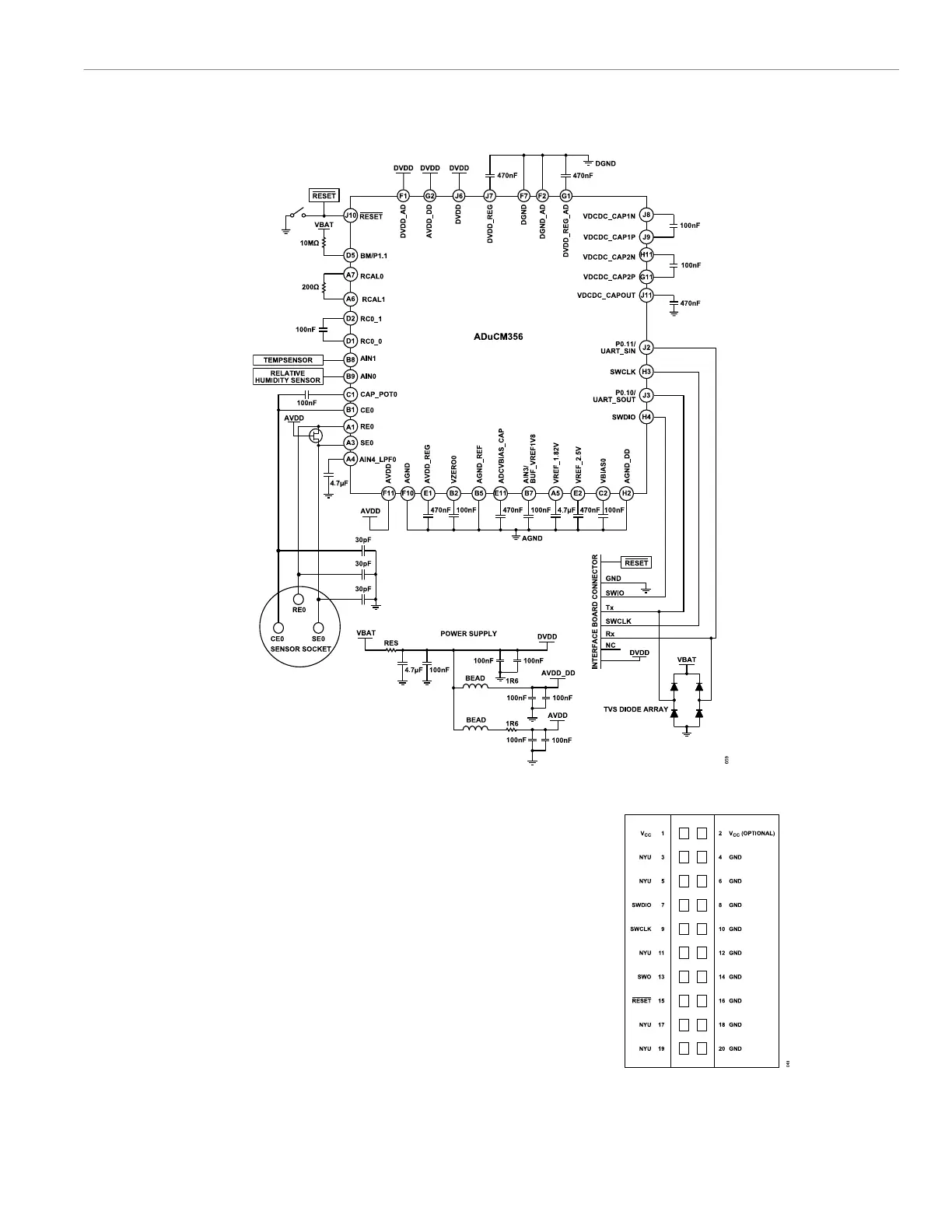
TYPICAL SYSTEM CONFIGURATION
Figure 67. ADuCM356 Typical System Configuration
SERIAL WIRE DEBUG INTERFACE
The SWD interface provides a debug port for pin limited packages.
The SWD replaces the 5-pin JTAG port with the SWCLK pin and a
single bidirectional data pin (SWDIO), providing all the normal JTAG
debug and test functionality. SWDIO and SWCLK are overlaid on
the TMS and TCK pins, respectively, on the Arm 20-pin JTAG
interface (see Figure 68).
Figure 68. SWD 20-Pin Connector Pinout
 Loading...