Reference Manual ADuCM356
USE CASE CONFIGURATIONS
analog.com Rev. A | 151 of 312
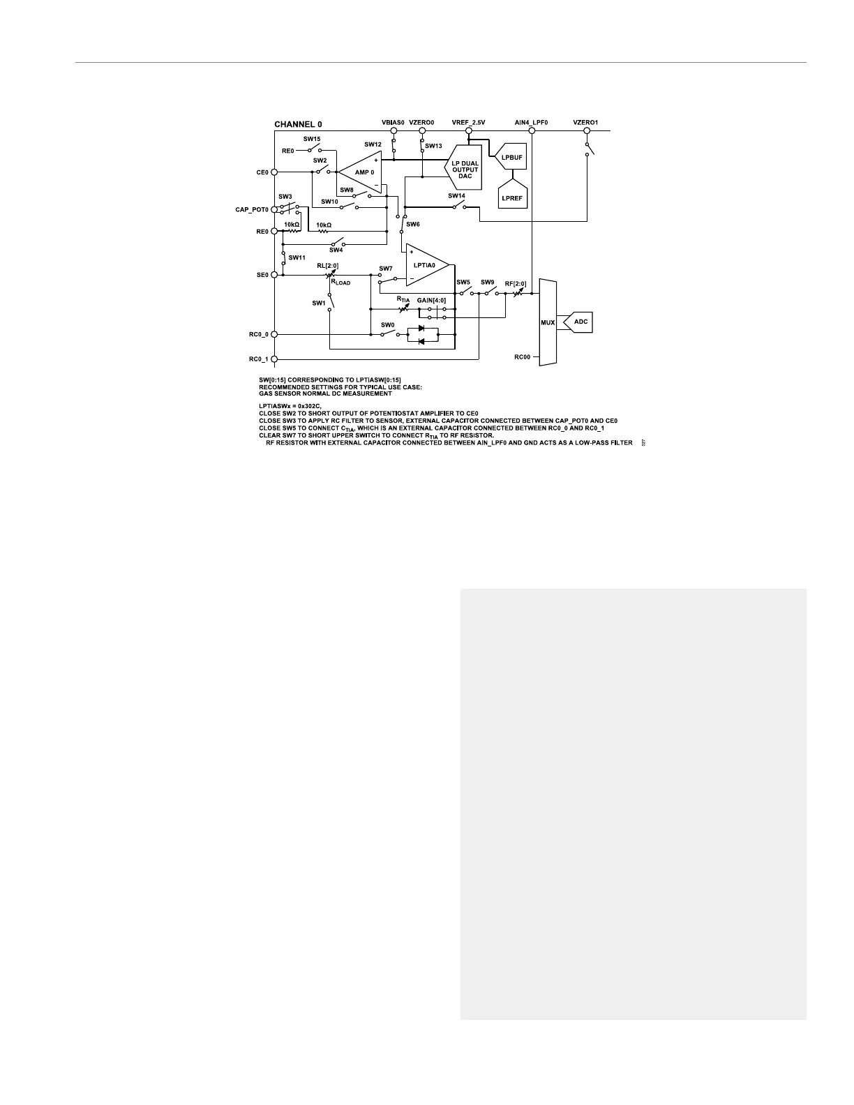
Figure 38. Switches for Low-Power Potentiostat Amplifier and Low-Power TIA to Measure DC Current from SE0 Node Using Low-Power TIA (3-Wire Electrochemical
Sensor Configuration)
PULSE TEST (CHRONOAMPEROMETRY)
The pulse test involves disturbing the normal bias voltage of an
electrochemical sensor and monitoring its output current response.
The pulse test is usually used to check the responsiveness of the
sensor. In the case of an electrochemical gas sensor, the pulse
test checks that the passage of charge between electrodes through
the internal electrolyte during oxidation and reduction is operating
properly. Typically, the current increases sharply and quickly with
the step in the sensor bias voltage. If the current step response is
slow, there can be an issue with the sensor electrolyte.
Implementing Pulse Test Using Low-Power TIA
The potentiostat and the ADC are assumed to be initially configured
using the steps in the Measuring a DC Current Output section.
Current measurement before, during, and after the step is also
described in this section.
The V
BIAS
DAC level is stepped by 5 mV to 10 mV higher than
it typically is to stimulate the sensor. A typical step duration is
100 ms.
To configure the switches in potentiostat mode for the pulse test,
set LPTIASWx, Bits[11:0] = 0x014 to use the low-power TIA, write
to the LPDACDAT0 register to change the VBIAS0 output voltage,
and write to the LPDACDAT1 register to change the VBIAS1 output
voltage.
Implementing Pulse Test Using High-Speed TIA
In this test, the user has the option of using the high-speed TIA
channel to measure the current of the sensor. In this case, the SE0
or SE1 pin is routed to the high-speed TIA instead of the low-power
TIA. Figure 40 shows the signal path.
The following code connects the SE0 pin to the high-speed TIA and
disconnects the SE0 pin from the low-power TIA0:
pADI_AFE->LPTIASW0 &= 0xF000; // Mask
SW12 to 15 control bits
pADI_AFE->LPTIASW0 = 0x94; // Dis►
connect SE from LPTIA -ve input and connect to
HSTIA
// Con►
figure SW0 to SW11 for HSTIA PULSE/RAMP test
setting
pADI_AFE->LPDACCON0 |= 0x20; // Con►
figure LPDAC0 switches for Diagnostic mode
pADI_AFE->LPDACSW0 = 0x32; // Dis►
connect the VBIAS0 and VZERO0 from external
caps
pADI_AFE->SWCON &=
(!BITM_AFE_SWCON_SWSOURCESEL); // Step
1: to write to T-Switch control register
pADI_AFE->TSWFULLCON = 0x110; // Step
2: Close T9 & T5. Leave T10, T11 open
pADI_AFE->SWCON |=
BITM_AFE_SWCON_SWSOURCESEL; // Step
3: to write to T-Switch control register
AfeHSTIACon(AMPPOWER_NORM,
HSTIABIAS_VZERO0); // Set common-
mode source as Vzero0 if HSTIA with Chan0
required
AfeHSTIASeCfg(HSTIA_RTIA_80K, // RTIA
 Loading...