EasyManua.ls Logo

Analog Devices ADuCM356 User Manual

Analog Devices ADuCM356
312 pages
To Next Page IconTo Next Page
To Previous Page IconTo Previous Page
Page #264 background imageLoading...
Page #264 background image
Reference Manual ADuCM356
DIGITAL DIE GENERAL-PURPOSE TIMERS
analog.com Rev. A | 264 of 312
DIGITAL DIE GENERAL-PURPOSE TIMERS
FEATURES
The ADuCM356 digital die integrates three identical general-pur-
pose, 16-bit count up or count down timers: Timer 0, Timer 1, and
Timer 2. These timers can be clocked from the 32 kHz internal
low frequency oscillator, the PCLK, or the internal 26 MHz high
frequency oscillator. Clock sources can be scaled down using a
prescaler to 1, 4, 16, or 256. Free running mode and periodic mode
are available. The timers have a capture events feature, with the
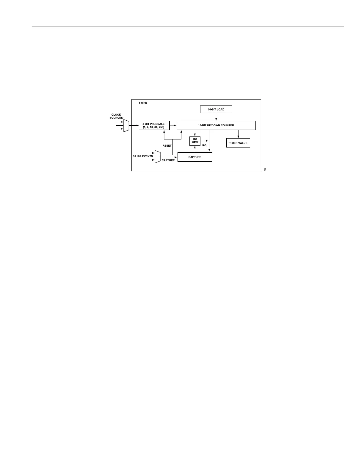
capability to capture 32 different events on each timer. See Figure
64 for an overview of the general-purpose timers.
Figure 64. General-Purpose Timers Block Diagram
GENERAL-PURPOSE TIMERS OVERVIEW
The timers can either be in free running mode or periodic mode. In
free running mode, the counter decrements from full scale to zero
scale or increments from zero scale to full scale and then restarts.
In periodic mode, the counter decrements or increments from the
value in the load register (GPTx_LOAD, where x is 0 for Timer 0,
1 for Timer 1, and 2 for Timer 2) until zero scale or full scale is
reached. The counter then restarts at the value stored in the load
register.
The value of a counter can be read at any time by access-
ing its value register, GPTx_ACURCNT or GPTx_CURCNT.
GPTx_ACURCNT assumes the timer and the CPU are synchron-
ized (using the same clock source). Do not use GPTx_ACURCNT if
the timer is using a different clock source, such as the low frequen-
cy oscillator. In this case, use GPTx_CURCNT. GPTx_CURCNT
returns a synchronized timer value but has a slightly delayed result
owing to the synchronization period required.
The CON0 register selects the timer mode, configures the clock
source, selects count up or count down, starts the counter, and
controls the event capture function.
An interrupt signal is generated each time the value of the counter
reaches 0 when counting down or each time the counter value
reaches the maximum value when counting up. Clear an IRQ by
writing 1 to the time clear interrupt register of that particular timer
(GPTx_CLRINT).
In addition, Timer 0, Timer 1, and Timer 2 have a capture register
that is triggered by a selected IRQ source initial assertion. When
triggered, the current timer value is copied to the GPTx_CAPTURE
register, and the timer continues to run. This feature determines the
assertion of an event with increased accuracy.
GENERAL-PURPOSE TIMER OPERATIONS
Free Running Mode
In free running mode, the timer is started by setting the enable bit
(GPTx_CTL, Bit 4) to 1 and the mode bit (GPTx_CTL, Bit 3) to 0.
The timer increments from zero scale or full scale to full scale or
zero scale if counting up or down. Full scale is 216, which is 1 or
0xFFFF. Upon reaching full scale or zero scale, a timeout interrupt
occurs and GPTx_STAT, Bit 0 is set. To clear the timer interrupt,
user code must write 1 to GPTx_CLRINT, Bit 0. If GPTx_CTL, Bit 7
is set, the timer keeps counting and reloads when GPTx_CLRINT,
Bit 0 is set to 1.
Periodic Mode
In periodic mode, the initial GPTx_LOAD value must be loaded be-
fore starting the timer by setting the enable bit (GPTx_CTL, Bit 4) to
1. The timer value either increments from the value in GPTx_LOAD
to full scale or decrements from the value in GPTx_LOAD to zero
scale, depending on the GPTx_CTL, Bit 2 settings (count up or
down). Upon reaching full scale or zero scale, the timer generates
an interrupt. GPTx_LOAD is reloaded into GPTx_CURCNT, and the
timer continues counting up or down. The timer must be disabled
prior to changing the GPTx_CTL or GPTx_LOAD register. If the
GPTx_LOAD register is changed while the timer is being loaded,
undefined results can occur. By default, the counter is reloaded
automatically when generating the interrupt signal. If GPTx_CTL,
Bit 7 is set to 1, the counter is also reloaded when user code writes
GPTx_CLRINT, which allows user changes to GPTx_LOAD to take
effect immediately instead of waiting until the next timeout.
The timer interval is calculated as follows:
If the timer is set to count down,

Table of Contents

Question and Answer IconNeed help?

Do you have a question about the Analog Devices ADuCM356 and is the answer not in the manual?

Analog Devices ADuCM356 Specifications

General IconGeneral
BrandAnalog Devices
ModelADuCM356
CategoryMicrocontrollers
LanguageEnglish

Summary

PREFACE

SCOPE

Provides a detailed description of the functionality and features of the ADuCM356.

CLOCKING ARCHITECTURE

DIGITAL DIE CLOCK FEATURES

Details the clock sources, dividers, and gating for the digital die system clock.

ANALOG DIE CLOCK FEATURES

Details the clock sources, dividers, and gating for the analog die system clock.

POWER MANAGEMENT UNIT

Active Mode

Describes the fully active operating mode where the Arm Cortex-M3 executes from flash and SRAM.

Flexi Mode

Describes the mode where the Arm Cortex-M3 is disabled, allowing peripherals to operate.

Hibernate Mode

Describes the low-power mode where the digital core and most analog blocks are powered down.

SYSTEM RESETS

DIGITAL DIE RESET OPERATION

Explains the reset sources and operation for the digital die, including software resets.

PROGRAMMING, PROTECTION, AND DEBUG

Debug Features

Details the SWD port, flash patch breakpoints, and data watchpoint/trigger units for debugging.

SYSTEM EXCEPTIONS AND PERIPHERAL INTERRUPTS

CORTEX-M3 AND FAULT MANAGEMENT

Describes the system exceptions and fault handling features integrated with the Cortex-M3 processor.

ANALOG DIE CIRCUITRY SUMMARY

ADC, HIGH-SPEED DAC, AND ASSOCIATED AMPLIFIERS OPERATING MODE CONFIGURATION

Configures the operating modes for ADC, High-Speed DAC, and associated amplifiers.

ADC CIRCUIT

ADC CIRCUIT FEATURES

Lists the key features of the ADuCM356's fast multichannel, 16-bit ADC.

LOW-POWER POTENTIOSTAT AMPLIFIERS AND LOW-POWER TIAS

LOW-POWER POTENTIOSTAT AMPLIFIERS

Details the two low-power potentiostat amplifiers for setting external sensor bias voltage.

HIGH-SPEED DAC CIRCUITS

HIGH-SPEED DAC OUTPUT SIGNAL GENERATION

Explains how to generate high-speed DAC output voltage via direct write or waveform generator.

PROGRAMMABLE SWITCHES CONNECTING THE EXTERNAL SENSOR TO THE HIGH-SPEED DAC AND HIGH-SPEED TIA

DX SWITCHES

Selects pins for the high-speed DAC excitation amplifier output, used for impedance measurements.

SEQUENCER

SEQUENCER COMMANDS

Describes the two types of commands: write commands and timer commands (wait, timeout).

SLEEP AND WAKE-UP TIMER

CONFIGURING A DEFINED SEQUENCE ORDER

Defines the order of sequence execution periodically using the SEQORDER register.

USE CASE CONFIGURATIONS

HIBERNATE MODE WHILE MAINTAINING A DC BIAS TO THE SENSOR

Details setup for hibernate mode while maintaining sensor bias voltage.

DMA CONTROLLER

DMA FEATURES

Lists the features of the ADuCM356's dedicated and independent DMA channels.

FLASH CONTROLLER

SUPPORTED COMMANDS

Summarizes the commands supported by the flash controller for read, write, erase, and signature operations.

REGISTER DETAILS: FLASH CACHE CONTROLLER (FLCC)

COMMAND REGISTER

Allows execution of specified flash commands like write, erase, abort, and signature generation.

DIGITAL INPUTS AND OUTPUTS

DIGITAL INPUTS AND OUTPUTS OPERATION

Explains how to configure, read, and write digital input and output pins.

I2C SERIAL INTERFACE

I2C OPERATION

Details the steps required to run the I2C peripheral, including startup and modes.

SERIAL PERIPHERAL INTERFACES

SPI OPERATION

Describes the operation of the SPI interface, including initiator and target modes.

REGISTER SUMMARY: SPI0/SPI1

STATUS REGISTERS

Provides status information for SPI0 and SPI1, including ready, overflow, and error conditions.

REGISTER DETAILS: UART

INTERRUPT ENABLE REGISTER

Configures which interrupt sources generate an interrupt for the UART.

DIGITAL DIE GENERAL-PURPOSE TIMERS

GENERAL-PURPOSE TIMER OPERATIONS

Explains the operation of timers in free running mode and periodic mode.

REGISTER SUMMARY: ANALOG DIE GENERAL-PURPOSE TIMERS

CONTROL REGISTER

Controls timer operation, including clock source, mode, and event selection.

REGISTER DETAILS: DIGITAL DIE WAKE-UP TIMER

STATUS 0 REGISTER

Provides status information for WUT operation, including synchronization and pending writes.

CYCLIC REDUNDANCY CHECK

CRC OPERATING MODES

Details the core access and DMA access modes for CRC calculation.

REGISTER SUMMARY: CRC

CRC CONTROL REGISTER

Controls the CRC peripheral, including enabling, mirroring, and calculation order.

HARDWARE DESIGN CONSIDERATIONS

SERIAL WIRE DEBUG INTERFACE

Describes the SWD interface for debugging and programming, replacing JTAG.