Reference Manual ADuCM356
DIGITAL INPUTS AND OUTPUTS
analog.com Rev. A | 211 of 312
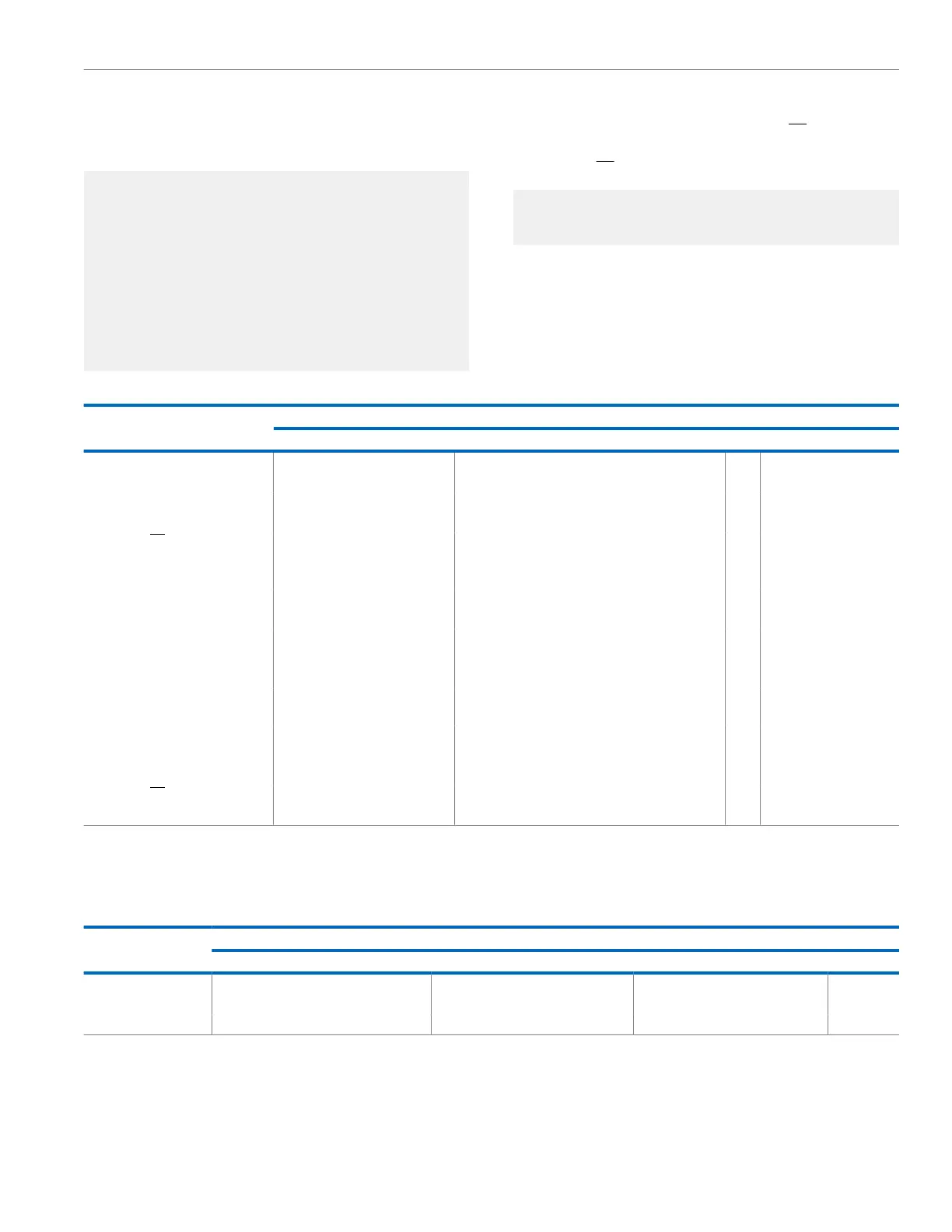
The following is example code for the GPIO pin interrupt handler
routine:
void GPIO_A_Int_Handler()
{
unsigned int uiIntSta = 0;
uiIntSta = pADI_GPIO1->INT;
if ((uiIntSta & 0x2) ==0x2) // interrupt
expected on P1.1
{
pADI_GPIO1->INT |= 0x2;
}
}
The following is example code to set P0.3/SPI0_CS as an output.
Write to GP0OUT, GP0SET, GP0CLR, and GP0TGL to set the level
on P0.3/SPI0_CS:
pADI_GPIO0->OEN |= 0x8; //
Configure P0.3 as an output
DIGITAL DIE PORT MUX
This block provides control over the GPIO functionality of specified
pins. Some pins have the ability to work as a GPIO or perform other
specific functions. Only configuration of the P2.4 pin of Port 2 is
permitted. Attempted writes to other port pins are not allowed. Any
blank cells in Table 255 are not applicable.
Table 255. GPIO Multiplex Table
GPIO Pin
Configuration Modes
00 01 10 11
GP0 (GP0CON Controls These Bits)
P0.0/SPI0_CLK GPIO (GP0CON, Bits[1:0] = 0x0) SPI0 serial clock (SCLK) (GP0CON, Bits[1:0] = 0x1)
P0.1/SPI0_MOSI GPIO (GP0CON, Bits[3:2] = 0x0) SPI0 MOSI (GP0CON, Bits[3:2] = 0x1)
P0.2/SPI0_MISO GPIO (GP0CON, Bits[5:4] = 0x0) SPI0 MISO (GP0CON, Bits[5:4] = 0x1)
P0.3/SPI0_CS GPIO (GP0CON, Bits[7:6] = 0x0) SPI0 chip select (GP0CON, Bits[7:6] = 0x1) SPI1 ready (GP0CON,
Bits[7:6] = 0x3)
P0.4/I2C_SCL GPIO (GP0CON, Bits[9:8] = 0x0) I2C I2C_SCL (GP0CON, Bits[9:8] = 0x1)
P0.5/I2C_SDA GPIO (GP0CON, Bits[11:10] = 0x0) I2C I2C_SDA (GP0CON, Bits[11:10] = 0x1)
P0.10/UART_SOUT GPIO (GP0CON, Bits[21:20] = 0x0) UART SOUT pin (GP0CON, Bits[21:20] = 0x1)
P0.11/UART_SIN GPIO (GP0CON, Bits[23:22] = 0x0) UART SIN pin (GP0CON, Bits[23:22] = 0x1)
GP1 (GP1CON Controls These Bits)
P1.0/SYS_WAKE GPIO (GP1CON, Bits[1:0] = 0x0)
BM/P1.1 GPIO boot (GP1CON, Bits[3:2] =
0x0)
GPIO (GP1CON, Bits[3:2] = 0x1)
P1.2/SPI1_CLK GPIO (GP1CON, Bits[5:4] = 0x0) SPI1 SCLK (GP1CON, Bits[5:4] = 0x1)
P1.3/SPI1_MOSI GPIO (GP1CON, Bits[7:6] = 0x0) SPI1 MOSI (GP1CON, Bits[7:6] = 0x1)
P1.4/SPI1_MISO GPIO (GP1CON, Bits[9:8] = 0x0) SPI1 MISO (GP1CON, Bits[9:8] = 0x1)
P1.5/SPI1_CS GPIO (GP1CON, Bits[11:10] = 0x0) SPI1 chip select (GP1CON, Bits[11:10] = 0x1)
P2.4 GPIO (GP2CON, Bits[9:8] = 0x0)
AFE DIE DIGITAL PORT MUX
This block provides control over the three digital die GPIO pins.
Two of these pins are bonded out as GPIO0/PWM0 and GPIO1/
PWM1. The third pin, referred to as P2.2, is an internal pin bonded
to the digital die P0.10/UART_SOUT pin and supports connecting
the AFE die system clock to the digital die.
Table 256. AFE Die GPIO Mux Table
GPIO
Configuration Modes (GP2CON Controls These Bits)
00 01 10 11
GPIO0 Reserved PWM0 (GP2CON, Bits[1:0] = 0x1) GPIO (GP2CON, Bits[1:0] = 0x2) Reserved
GPIO1 Reserved PWM1 (GP2CON, Bits[3:2] = 0x1) GPIO (GP2CON, Bits[3:2] = 0x2) Reserved
P2.2 (Internal Only) CLK_OUT (GP2CON, Bits[5:4] = 0x0) Reserved Reserved Reserved
 Loading...