Reference Manual ADuCM356
I
2
C SERIAL INTERFACE
analog.com Rev. A | 223 of 312
In initiator mode, the steps are as follows:
1. Clear MCTL, Bit 0 to 0 and disable the I
2
C initiator.
2. Set SHCTL, Bit 0 to 1, which is a write only register. Writing
to this bit resets the start and stop detection circuits of the I
2
C
block and clears MSTAT, Bit 10.
3. Set MCTL, Bit 0 to 1 to reenable the I
2
C initiator.
In target mode, the steps are as follows:
1. Clear SCTL, Bit 0 to 0 and disable the I
2
C target.
2. Set SHCTL, Bit 0 to 1, which is a write only register. Writing
to this bit resets the start and stop detection circuits of the I
2
C
block.
3. Set SCTL, Bit 0 to 1 to reenable the I
2
C target.
I
2
C OPERATING MODES
Initiator Transfer Initiation
If the initiator enable bit (MCTL, Bit 0) is set, an initiator transfer
sequence is initiated by writing a value to the ADR1 register. If there
is valid data in the MTX register, it is the first byte transferred in the
sequence after the address byte during a write sequence.
Target Transfer Initiation
If the target enable bit (SCTL, Bit 0) is set, a target transfer
sequence is monitored for the device address in Register ID0,
Register ID1, Register ID2, or Register ID3. If the device address is
recognized, the device participates in the target transfer sequence.
Note that a target operation always starts with the assertion of one
of three interrupt sources: a read request (MRXREQ, SRXREQ),
a write request (MTXREQ, STXREQ), or a general call interrupt
(GCINT). The software must always look for a stop interrupt to
ensure that the transaction has completed correctly and to deassert
the stop interrupt status bit.
Receive and Transmit Data FIFOs
The transmit data path consists of an initiator and target transmit
FIFO (each two bytes deep), the MTX register and STX register,
and a transmit shifter. The transmit status bits, MSTAT, Bits[1:0],
and SSTAT, Bit 0 denote whether there is valid data in the transmit
FIFO. Data from the transmit FIFO is loaded into the transmit shifter
when a serial byte begins transmission. If the transmit FIFO is
not full during an active transfer sequence, the transmit request
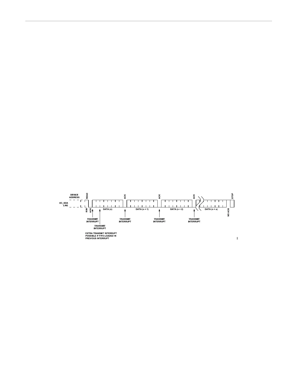
bit (MSTAT, Bit 2 or SSTAT, Bit 2) asserts. Figure 60 shows the
effect of not having the target transmit FIFO full at the start of a
read request from an initiator. An extra transmit interrupt can be
generated after the read bit. This extra transmit interrupt occurs if
the transmit FIFO is not full.
Figure 60. I
2
C Target Transmit Interrupt Details
In the target, if there is no valid data to transmit when the transmit
shifter is loaded, the transmit underflow status bit asserts (MSTAT,
Bit 12 or SSTAT, Bit 1). In target mode, the transmit FIFO must be
loaded with a byte before the falling edge of I2C_SCL and before
the acknowledge or no acknowledge is asserted. If the transmit
FIFO is empty on the falling edge of I2C_SCL for an R/W bit, the
target returns a no acknowledge because the target in this case
controls the acknowledge or no acknowledge.
If the first byte is transmitted correctly in a target transmit sequence,
but the transmit FIFO is empty for any subsequent bytes in the
same transfer, the target returns the previous transmitted byte. This
operation is due to the initiator having control of the acknowledge
or no acknowledge during a target transfer sequence. The initiator
generates a stop condition if there is no data in the transmit FIFO
and the initiator is writing data.
The receive data path consists of an initiator and target receive
FIFO, the MRX register, and the SRX register. Both are two bytes
deep. The receive request interrupt bit (MSTAT, Bit 3 or SSTAT, Bit
3) indicates whether there is valid data in the receive FIFO. Data
is loaded into the receive FIFO after each byte is received. If valid
data in the receive FIFO is overwritten by the receive shifter, the
receive overflow status bit is asserted (MSTAT, Bit 9 or SSTAT, Bit
4).
Automatic Clock Stretching
The ASTRETCH_SCL register controls automatic clock stretching.
If automatic clock stretching is enabled, the I
2
C hardware holds
the I2C_SCL pin low after the falling edge of I2C_SCL before an
acknowledge or no acknowledge under the following conditions:
 Loading...