EasyManua.ls Logo

Analog Devices ADuCM356 User Manual

Analog Devices ADuCM356
312 pages
To Next Page IconTo Next Page
To Previous Page IconTo Previous Page
Page #161 background imageLoading...
Page #161 background image
Reference Manual ADuCM356
DMA CONTROLLER
analog.com Rev. A | 161 of 312
DMA OPERATING MODES
The DMA controller has two buses, one connected to the system
bus shared with the Cortex-M3 core and the other connected to
16-bit peripherals. The DMA request can stop CPU access to the
system bus for several bus cycles, such as when the CPU and
DMA target the same destination (memory or peripheral). The DMA
controller fetches channel control data structures located in the
system memory to perform data transfers.
DMA capable peripherals, when enabled to use the DMA, can
request the DMA controller for a transfer. At the end of the program-
med number of DMA transfers for a channel, the DMA controller
generates a single cycle DMA_DONE interrupt corresponding to
that channel. The DMA_DONE interrupt indicates the completion of
the DMA transfer. Separate interrupt enable bits are available in the
NVIC for each of the DMA channels.
CHANNEL CONTROL DATA STRUCTURE
Every channel has two associated control data structures: primary
and alternate. For simple transfer modes, the DMA controller uses
either the primary or the alternate data structure. For more complex
data transfer modes, such as ping pong or scatter gather, the DMA
controller uses both the primary and alternate data structures. Both
control data structures occupy four 32-bit locations in the memory,
as detailed in Table 189. The entire channel control data structure is
described in Table 190.
Before the controller can perform a DMA transfer, the data structure
related to the DMA channel must be programmed at the designated
location in system memory, SRAM. The programming determines
the source and destination data size, number of transfers, and the
number of arbitrations. The contents of the designated memory
locations are as follows:
â–º The source end pointer memory location contains the end ad-
dress of the source data.
â–º The destination end pointer memory location contains the end
address of the destination data.
â–º The control data configuration memory location contains the
channel configuration control data.
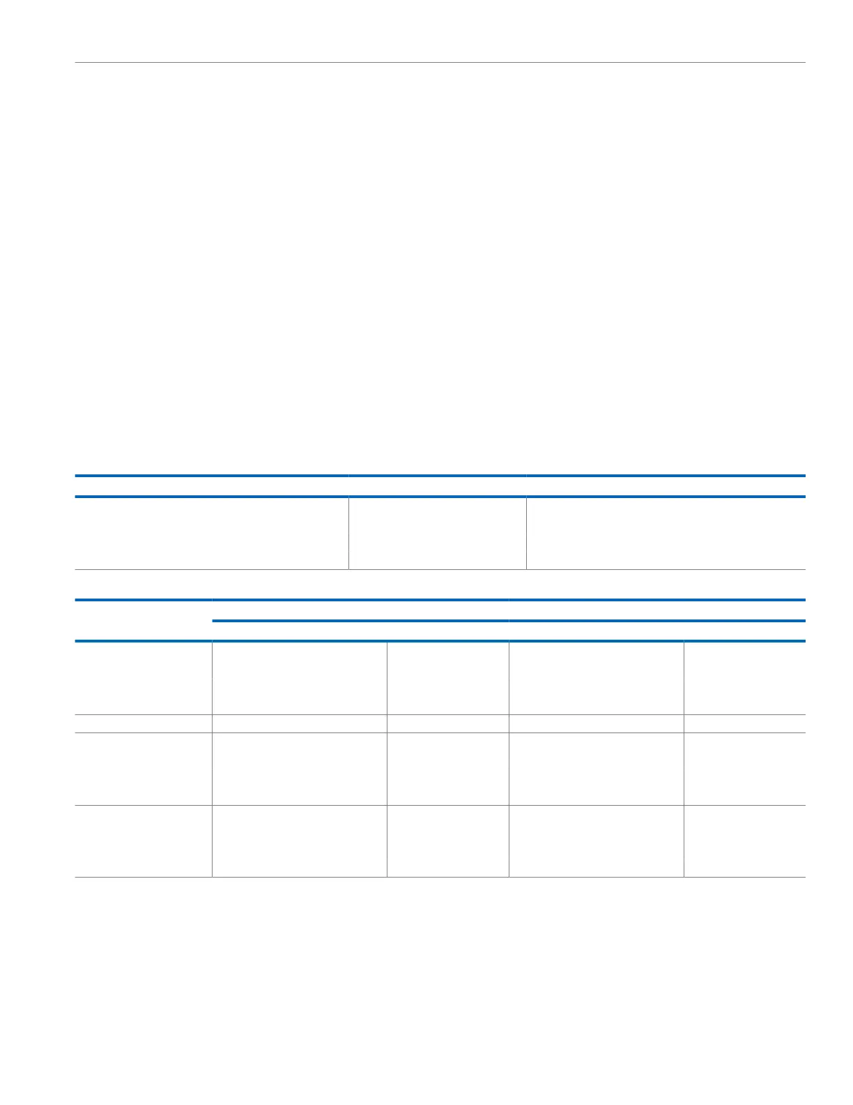
Table 189. Channel Control Data Structure
Offset Address Offset Register Name Description
0x00 SRC_END_PTR Source end pointer
0x04 DST_END_PTR Destination end pointer
0x08 CHNL_CFG Control data configuration
0x0C Reserved Reserved
Table 190. Memory Map of Primary and Alternate DMA Structures
1
Channel Number
Primary Structures Alternate Structures
Register Description Offset Address Register Description Offset Address
Channel 23 Reserved, set to 0 0x17C Reserved, set to 0 0x1DC
Control 0x178 Control 0x1D8
Destination end pointer 0x174 Destination end pointer 0x1D4
Source end pointer 0x170 Source end pointer 0x1D0
… … … … …
Channel 1 Reserved, set to 0 0x01C Reserved, set to 0 0x11C
Control 0x018 Control 0x118
Destination end pointer 0x014 Destination end pointer 0x114
Source end pointer 0x010 Source end pointer 0x110
Channel 0 Reserved, set to 0 0x00C Reserved, set to 0 0x10C
Control 0x008 Control 0x108
Destination end pointer 0x004 Destination end pointer 0x104
Source end pointer 0x000 Source end pointer 0x100
1
The row with ellipses (…) indicates all channels between Channel 23 and Channel 1. These channels follow the same register naming contentions and offset address
pattern.
The user must define the DMA structures in their source code, as
shown in the Example Code: Define DMA Structures section. After
the structure has been defined, its start address must be assigned
to the DMA base address pointer register, PDBPTR. Each register
for each DMA channel is then at the offset address (as specified in
Table 190) plus the value in the PDBPTR register.
When the DMA controller receives a request for a channel, it reads
the corresponding data structure from the system memory into its
internal cache. Any update to the descriptor in the system memory

Table of Contents

Question and Answer IconNeed help?

Do you have a question about the Analog Devices ADuCM356 and is the answer not in the manual?

Analog Devices ADuCM356 Specifications

General IconGeneral
BrandAnalog Devices
ModelADuCM356
CategoryMicrocontrollers
LanguageEnglish

Summary

PREFACE

SCOPE

Provides a detailed description of the functionality and features of the ADuCM356.

CLOCKING ARCHITECTURE

DIGITAL DIE CLOCK FEATURES

Details the clock sources, dividers, and gating for the digital die system clock.

ANALOG DIE CLOCK FEATURES

Details the clock sources, dividers, and gating for the analog die system clock.

POWER MANAGEMENT UNIT

Active Mode

Describes the fully active operating mode where the Arm Cortex-M3 executes from flash and SRAM.

Flexi Mode

Describes the mode where the Arm Cortex-M3 is disabled, allowing peripherals to operate.

Hibernate Mode

Describes the low-power mode where the digital core and most analog blocks are powered down.

SYSTEM RESETS

DIGITAL DIE RESET OPERATION

Explains the reset sources and operation for the digital die, including software resets.

PROGRAMMING, PROTECTION, AND DEBUG

Debug Features

Details the SWD port, flash patch breakpoints, and data watchpoint/trigger units for debugging.

SYSTEM EXCEPTIONS AND PERIPHERAL INTERRUPTS

CORTEX-M3 AND FAULT MANAGEMENT

Describes the system exceptions and fault handling features integrated with the Cortex-M3 processor.

ANALOG DIE CIRCUITRY SUMMARY

ADC, HIGH-SPEED DAC, AND ASSOCIATED AMPLIFIERS OPERATING MODE CONFIGURATION

Configures the operating modes for ADC, High-Speed DAC, and associated amplifiers.

ADC CIRCUIT

ADC CIRCUIT FEATURES

Lists the key features of the ADuCM356's fast multichannel, 16-bit ADC.

LOW-POWER POTENTIOSTAT AMPLIFIERS AND LOW-POWER TIAS

LOW-POWER POTENTIOSTAT AMPLIFIERS

Details the two low-power potentiostat amplifiers for setting external sensor bias voltage.

HIGH-SPEED DAC CIRCUITS

HIGH-SPEED DAC OUTPUT SIGNAL GENERATION

Explains how to generate high-speed DAC output voltage via direct write or waveform generator.

PROGRAMMABLE SWITCHES CONNECTING THE EXTERNAL SENSOR TO THE HIGH-SPEED DAC AND HIGH-SPEED TIA

DX SWITCHES

Selects pins for the high-speed DAC excitation amplifier output, used for impedance measurements.

SEQUENCER

SEQUENCER COMMANDS

Describes the two types of commands: write commands and timer commands (wait, timeout).

SLEEP AND WAKE-UP TIMER

CONFIGURING A DEFINED SEQUENCE ORDER

Defines the order of sequence execution periodically using the SEQORDER register.

USE CASE CONFIGURATIONS

HIBERNATE MODE WHILE MAINTAINING A DC BIAS TO THE SENSOR

Details setup for hibernate mode while maintaining sensor bias voltage.

DMA CONTROLLER

DMA FEATURES

Lists the features of the ADuCM356's dedicated and independent DMA channels.

FLASH CONTROLLER

SUPPORTED COMMANDS

Summarizes the commands supported by the flash controller for read, write, erase, and signature operations.

REGISTER DETAILS: FLASH CACHE CONTROLLER (FLCC)

COMMAND REGISTER

Allows execution of specified flash commands like write, erase, abort, and signature generation.

DIGITAL INPUTS AND OUTPUTS

DIGITAL INPUTS AND OUTPUTS OPERATION

Explains how to configure, read, and write digital input and output pins.

I2C SERIAL INTERFACE

I2C OPERATION

Details the steps required to run the I2C peripheral, including startup and modes.

SERIAL PERIPHERAL INTERFACES

SPI OPERATION

Describes the operation of the SPI interface, including initiator and target modes.

REGISTER SUMMARY: SPI0/SPI1

STATUS REGISTERS

Provides status information for SPI0 and SPI1, including ready, overflow, and error conditions.

REGISTER DETAILS: UART

INTERRUPT ENABLE REGISTER

Configures which interrupt sources generate an interrupt for the UART.

DIGITAL DIE GENERAL-PURPOSE TIMERS

GENERAL-PURPOSE TIMER OPERATIONS

Explains the operation of timers in free running mode and periodic mode.

REGISTER SUMMARY: ANALOG DIE GENERAL-PURPOSE TIMERS

CONTROL REGISTER

Controls timer operation, including clock source, mode, and event selection.

REGISTER DETAILS: DIGITAL DIE WAKE-UP TIMER

STATUS 0 REGISTER

Provides status information for WUT operation, including synchronization and pending writes.

CYCLIC REDUNDANCY CHECK

CRC OPERATING MODES

Details the core access and DMA access modes for CRC calculation.

REGISTER SUMMARY: CRC

CRC CONTROL REGISTER

Controls the CRC peripheral, including enabling, mirroring, and calculation order.

HARDWARE DESIGN CONSIDERATIONS

SERIAL WIRE DEBUG INTERFACE

Describes the SWD interface for debugging and programming, replacing JTAG.