Reference Manual ADuCM356
ADC CIRCUIT
analog.com Rev. A | 55 of 312
ADC LOW-POWER CURRENT INPUT
CHANNELS
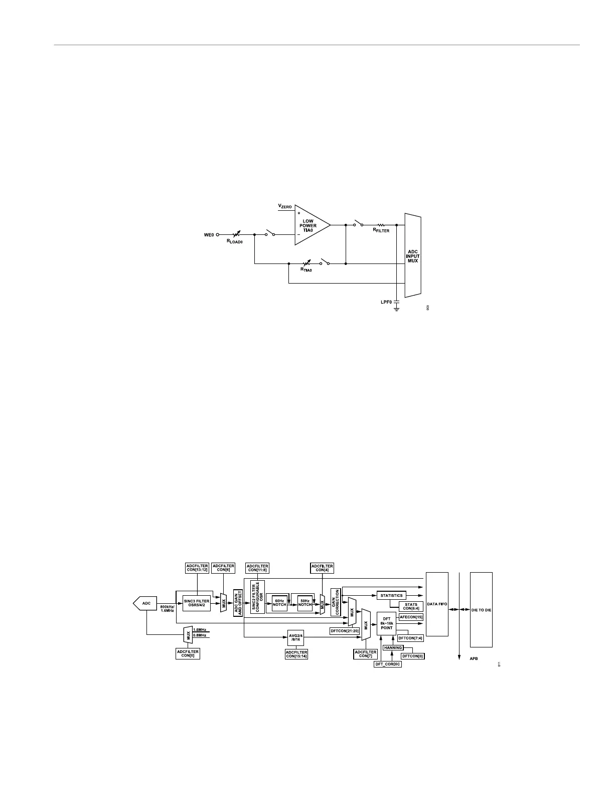
Figure 10 shows the low-power TIA0 input current channel, low-
power TIA0. The low-power TIA1 input current channel, low-power
TIA1, is identical to low-power TIA0. The output of the low-power
TIA is the voltage proportional to the input current measured by the
ADC. Details on how to configure the R
LOAD0
resistor, R
TIA0
resistor,
and low-pass filter programmable resistor (R
FILTER
) values can be
found in the Low-Power TIAs section.
To select the low-power TIA input channel for calibration and meas-
urement, refer to ADCCON, Bits[12:0] in Table 63. For low-power
TIA0, the ADC positive input is selected by setting ADCCON,
Bits[5:0] = 0b000010. For low power TIA1, the ADC positive input is
selected by setting ADCCON, Bits[5:0] = 0b000011.
Figure 10 also shows the low-power DAC (V
ZERO
) signal controlling
the low-power TIA positive input voltage level.
Figure 10. Low-Power TIA0 Current Input Channel to the ADC
The low-power TIA outputs have a low-pass filter. The resistor
connecting the TIA output to the input mux is typically 1 MΩ with
a recommended external low-pass filter capacity of 4.7 μF resulting
in a very low cutoff frequency. This resistor is labeled RFILTER
in Figure 10. For more details on how to set up the sensor bias
voltage, see the Low-Power DACs section.
ADC INPUT CIRCUIT
Figure 8 shows a basic view of the ADC input stages from the ADC
mux to the ADC.
The ADC input mux is programmable to select from up to 34
positive input channels. Features of the input mux include the
following:
► The positive input can be selected via ADCCON, Bits[5:0].
► The negative input is nominally expected to be the 1.11 V
reference source, selected via ADCCON, Bits[12:8] = 0b01000.
► An optional PGA can be selected to amplify the positive voltage
input. The PGA or instrumentation amplifier are enabled via
AFECON, Bit 10. The gain setting is configured via ADCCON,
Bits[18:16].
► The output of the gain stage goes through an antialias filter. The
cutoff frequency of the antialias filter is set by PMBW, Bits[3:2].
Set the cutoff frequency to suit the input signal bandwidth. See
the ADC, High-Speed DAC, and Associated Amplifiers Operating
Mode Configuration section for more details.
The ADC output code is calibrated with an offset and gain correc-
tion factor. This digital adjustment factor occurs automatically. The
offset and gain correction register used depends on the ADC input
channel selected. See the ADC Calibration section for more details.
ADC POSTPROCESSING FILTER OPTIONS
Figure 11 shows an overview of the postprocessing options for ADC
results.
Figure 11. ADC Postprocessing Filter Options
 Loading...