Reference Manual ADuCM356
DIGITAL INPUTS AND OUTPUTS
analog.com Rev. A | 209 of 312
DIGITAL INPUTS AND OUTPUTS FEATURES
The ADuCM356 features multiple bidirectional GPIO pins (GPIOx/
PWMx). Most of the GPIO pins have multiple functions, configura-
ble by user code. On power-up, these pins are configured as
tristate. There are three 16-bit wide ports. However, not all bits
on some ports are accessible. Ignore inaccessible bits. All GPIO
port pins provide input interrupt functionality. A typical GPIO pin
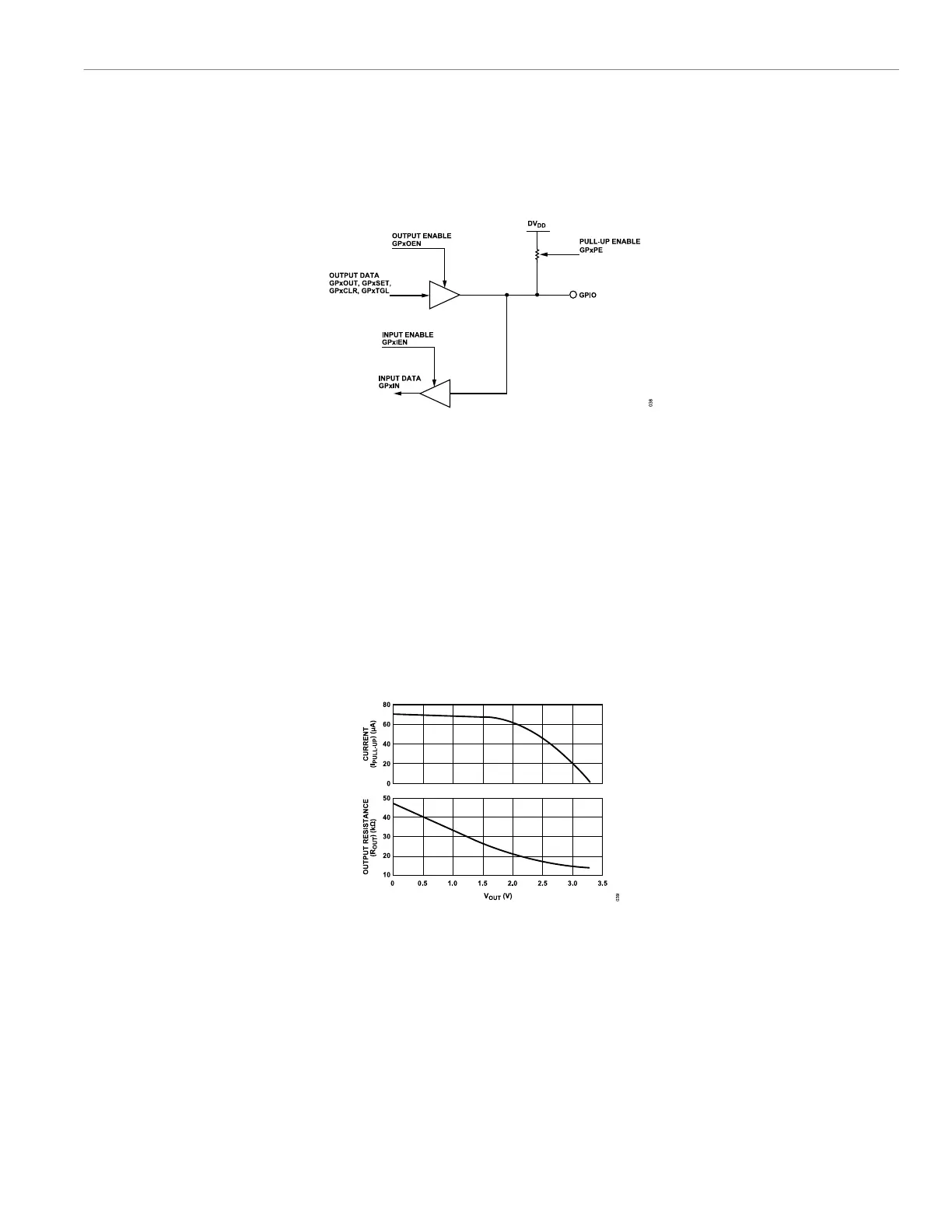
structure is shown in Figure 55.
Figure 55. GPIO Structure for Pins with Pull-Up Resistors
DIGITAL INPUTS AND OUTPUTS OVERVIEW
The GPIOs are grouped into three ports, Port 0, Port 1, and Port
2. Each GPIO can be configured as an input, output, or fully open
circuit. In input mode, the internal pull-up resistor or pull-down
resistor can be enabled by software. All input and output pins
are functional over the full supply range (DVDD = 2.8 V to 3.6 V
(maximum)), and the GPIO low input voltage (V
INL
) and GPIO high
input voltage (V
INH
) are specified as percentages of the supply as
follows:
V
INL
= 0.25 × DVDD maximum
(21)
V
INH
= 0.6 × DVDD minimum
(22)
The absolute maximum input voltage is DVDD + 0.3 V. The typical
leakage current of the GPIOs configured as input or open circuit
is 10 nA per GPIO. When the ADuCM356 enters a power saving
mode, the GPIO pins retain their states. In power saving mode, a
driving peripheral cannot drive the pin. If the UART is driving the pin
upon entry to deep sleep, it is isolated from the pin and power is
gated. Its state and control are restored upon wakeup.
Some of the bits of Port 0, Port 1, and Port 2 are not bonded out
of the package. The pin definitions in Table 255 indicate which are
accessible. The inaccessible bits are still implemented. By default,
these pins are tristate.
Figure 56. Typical Port 0, Port 1, and Port 2 Pull-Up Characteristics
DIGITAL INPUTS AND OUTPUTS OPERATION
Each digital input and output is configured, read, and written inde-
pendent of the other bits.
General-Purpose Input Data (GPxIN)
The status of the GPIO pins can be read via the GPxIN registers
when configured as inputs by the GPxIEN registers.
General-Purpose Output Data (GPxOUT)
The values of the GPxOUT registers are output on the GPIO pins
when configured as outputs by the GPxOEN registers.
Input/Output Data Out Enable (GPxOEN)
The GPxOEN registers enable the values of the GPxOUT registers
to be output on the GPIO pins.
 Loading...