Reference Manual ADuCM356
HIGH-SPEED TIA CIRCUITS
analog.com Rev. A | 99 of 312
Table 120. Configuration of R
LOAD
and R
TIA
of High-Speed TIA When Using DE0 and DE1 Electrodes (Continued)
DE0RESCON, Bits[7:0] (DE0) and DE1RESCON, Bits[7:0] (DE1) Setting R
LOAD03
and R
LOAD05
Value (Ω) R
TIA2_03
and R
TIA2_05
Value
0x1B 50 50 Ω
0x33 50 100 Ω
0x4B 50 190 Ω
0x5B 50 1.05 kΩ
0x63 50 5.05 kΩ
0x6B 50 10.05 kΩ
0x73 50 20.05 kΩ
0x7B 50 40.05 kΩ
0x83 50 80.05 kΩ
0x8B 50 160.05 kΩ
0x34 100 50 Ω
0x3C 100 100 Ω
0x54 100 200 Ω
0x5C 100 1 kΩ
0x64 100 5 kΩ
0x6C 100 10 kΩ
0x74 100 20 kΩ
0x7C 100 40 kΩ
0x84 100 80 kΩ
0x8C 100 160 kΩ
The high-speed TIA common-mode voltage setting (positive input
to the high-speed TIA amplifier) is configurable via HSTIACON,
Bits[1:0]. The configuration options are as follows:
► Internal 1.1 V reference source (same as ADCVBIAS_CAP pin
voltage).
► Sensor Channel 0 low-power DAC output (VZERO0 pin). See
Table 110 and Table 115 for details.
► Sensor Channel 1 low-power DAC output (VZERO1 pin). See
Table 112 and Table 118 for details.
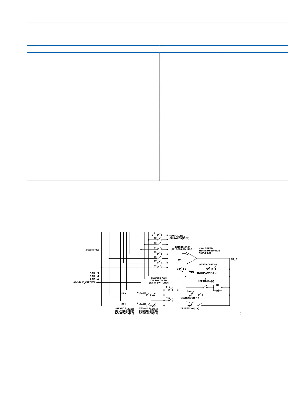
Figure 21 shows the high-speed TIA connections to external pins
and the programmable switch and resistor locations in this part of
the receive signal circuitry.
Figure 21. High-Speed TIA Circuitry
USING DE0 AND DE1 INPUTS WITH THE HIGH-
SPEED TIA
To use DE0 as the input of the high-speed TIA, set the following
register values:
► DE0RESCON = value required to set R
LOAD03
and R
TIA2_03
. See
Table 120.
► HSRTIACON, Bits[3:0] = 0xF to disconnect R
TIA2
from the high-
speed TIA.
 Loading...