Reference Manual ADuCM356
USE CASE CONFIGURATIONS
analog.com Rev. A | 149 of 312
Figure 37. Recommended Switch Settings to Minimize Leakage in Hibernate Mode of Unused AFE Circuits
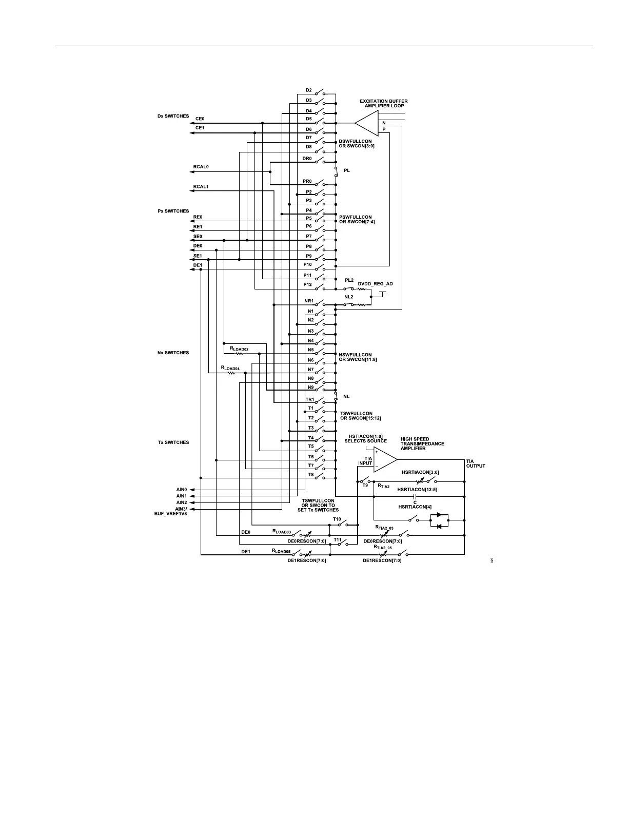
MEASURING A DC CURRENT OUTPUT
When measuring a DC current output, the ADC is powered on and
set to measure the low-power TIA input channel. The user has the
option to average the ADC results before reading to the digital die,
or to use DMA mode to directly move the ADC results to the digital
die SRAM.
Configure the Potentiostat Loop
Configure the low-power DACs to match the required sensor bias
voltage of the external electrochemical in use. For example, for a
sensor that requires a 0 V bias voltage between the working elec-
trode and reference electrode, the V
BIAS
and V
ZERO
DAC outputs
must be set to the same voltage. Likewise, LPDACDAT0 = 0x1A680
sets both VBIAS0 and VZERO0 outputs to approximately 1.1 V.
Additional guidelines are as follows:
► Configure the LPDACCON0 register as required. Set LPDAC-
CON0, Bit 5 = 0 for normal operation of the low-power DAC
switches.
► LPTIASW0, Bits[13:12] = 11 connects the V
BIAS
/V
ZERO
voltage
sources to an external capacitor for noise filtering purposes.
► Configure the other low-power potentiostat switches appropriate-
ly.
 Loading...