Reference Manual ADuCM356
CYCLIC REDUNDANCY CHECK
analog.com Rev. A | 303 of 312
The CRC accelerator on the digital die computes the CRC for a
block of memory locations on the digital die only. The exact memory
location can be in the SRAM, flash, or any combination of memory
mapped registers. The CRC accelerator generates a checksum
that can be compared to an expected signature. The final CRC
comparison is the responsibility of the MCU. CRC function is not
supported for the AFE die blocks.
CRC FEATURES
The CRC, used by the ADuCM356 MCU, supports the following
features:
► Generation of a CRC signature for a block of data.
► Programmable polynomial length of up to 32 bits.
► Operates on 32 bits of data at a time.
► MSB first and LSB first CRC implementations.
►
Various data mirroring capabilities.
► Initial seed to be programmed by user.
►
DMA controller (using software DMA) can be used for data
transfer to offload workload from the MCU.
CRC FUNCTIONAL DESCRIPTION
The following sections detail the functionality of the CRC. Control
for address decrementation and incrementation options for comput-
ing the CRC on a block of memory is in the DMA controller,
and details on these options can be found in the DMA Controller
section.
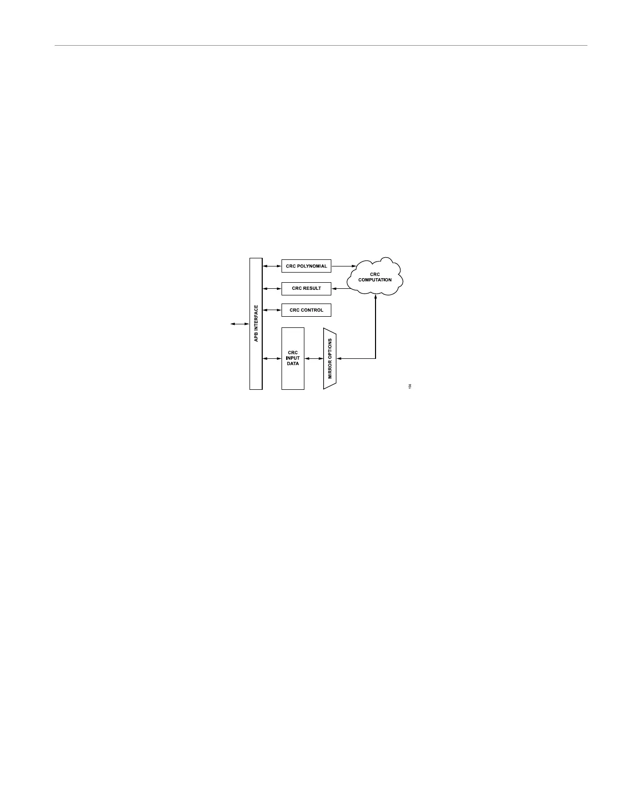
Figure 66. CRC Block Diagram
CRC Architectural Concepts
The CRC accelerator works on 32-bit data words, which are either
fed to the block through the DMA channel dedicated to the CRC ac-
celerator or directly by the MCU. The CRC accelerator guarantees
immediate availability of the CRC output.
CRC Operating Modes
The accelerator calculates CRC on the data stream it receives, 32
bits at a time. The CRC is then written into the block using either
the DMA engine or via the MCU directly.
The CRC works on 32-bit data words. For data words less than 32
bits in size, the MCU must pack the data into 32-bit data units. Data
mirroring on the input data can be performed at bit, byte, or word
level (only for 32-bit data) by setting CTL, Bits[4:2].
When operating, the CRC algorithm runs on the incoming data
stream written to the IPDATA register. For every new word of data
received, the CRC is computed and the result register is updated
with the calculated CRC. The CRC accelerator guarantees the
immediate availability of the CRC result up to the current data in the
result register.
The CRC engine uses the current result for generating the next
result when a new data word is received. The result register can
be programmed with an initial seed. The bit width of the seed value
for an x-bit polynomial must be x. The seed must be justified in the
result register.
Polynomial
The CRC accelerator supports the calculation of the CRC using any
length polynomial. The polynomial must be written to the polynomial
register. For MSB first implementation, omit the highest power
while programming the CRC polynomial register and left justify the
polynomial. For LSB first implementation, right justify the polynomial
and omit the LSB. The result register contains x-bit MSBs as a
checksum for an x-bit CRC polynomial.
The following examples illustrate the CRC polynomial.
16-Bit Polynomial Programming for MSB First
Calculation
Polynomial: CRC-16-CCITT
x
16
+ x
12
+ x
5
+ 1 = (1) 0001 0000 0010 0001 = 0x1021
where the largest exponent (x
16
term) is implied. Therefore, the
polynomial is 0001 0000 0010 0001.
When left justified in the polynomial register, the register format is
detailed in Table 397.
 Loading...