Reference Manual ADuCM356
SRAM
analog.com Rev. A | 200 of 312
This section provides an overview of the SRAM functionality of
the ADuCM356 processor. For details about the SRAM_INITSTAT,
SRAM_CTL, and SRAMRET registers, refer to the Register Sum-
mary: Power Management Unit section.
This memory space contains the application instructions and con-
stant data that must be executed in real time. It supports read
and write access via the Cortex-M3 core and read and write DMA
access by system peripherals. SRAM is divided into data SRAM
of 32 kB and instruction SRAM of 32 kB. If instruction SRAM is
not enabled, the associated 32 kB can be mapped as data SRAM,
resulting in a 64 kB data SRAM.
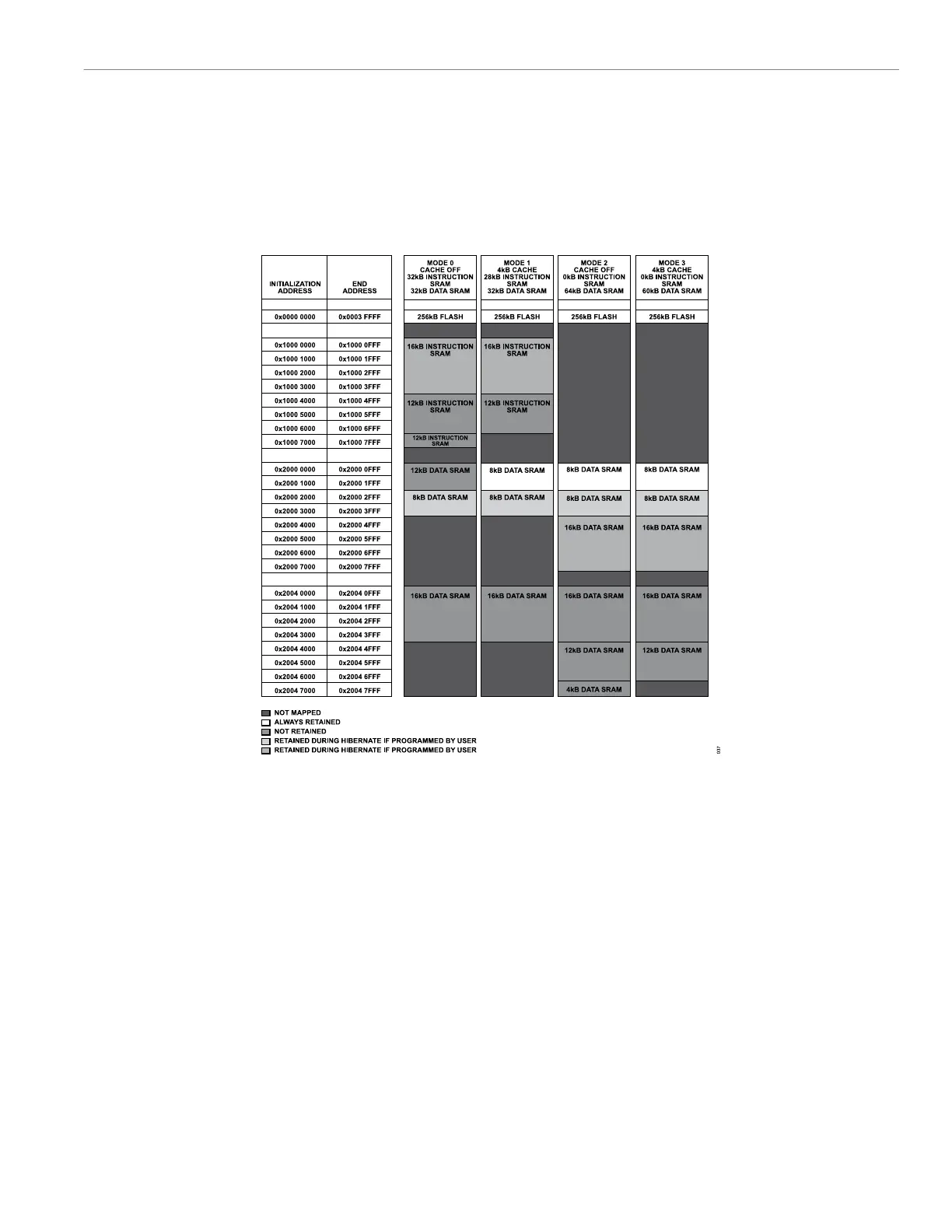
Figure 54. ADuCM356 SRAM Memory Details
SRAM FEATURES
The SRAM used by the ADuCM356 processor supports the follow-
ing features:
► Low-power controller for data SRAM, instruction SRAM, and
cache SRAM.
► Total available memory: 64 kB.
► Maximum retained memory in hibernate mode: 32 kB.
► The data SRAM is composed of 32 kB. There is an option to
retain 8 kB or 16 kB in hibernate mode.
► The instruction SRAM is composed of 32 kB. There is an option
to retain 16 kB in hibernate mode.
► If instruction SRAM is not enabled, the associated 32 kB can be
mapped as data SRAM. In this case, there is the option to retain
8 kB, 16 kB, 24 kB, or 32 kB of data SRAM.
► When the cache controller is enabled, 4 kB of the instruction
SRAM is reserved for cache data. Those 4 kB of cache data are
not retained in hibernate mode.
► Parity bit error detection (optional) is available on all SRAM
memories. Two parity bits are associated with each 32-bit word.
Parity check can be configured to be enabled or disabled in
different memory regions. Parity is on by default.
► Byte, half word, and word accesses are supported.
INSTRUCTION VS. DATA SRAM
If SRAM_CTL, Bit 31 is asserted, 32 kB of SRAM is mapped at
Start Address 0x10000000 as two 16 kB instruction SRAMs (see
Mode 0 and Mode 1 in Figure 54). The 32 kB of data SRAM is
mapped in two sections, the first starting at 0x20000000 and the
second starting at 0x20040000. If the cache memory feature is
used, only 28 kB are available for instruction SRAM (see Mode 1 in
Figure 54).
 Loading...