EasyManua.ls Logo

Analog Devices ADuCM356 User Manual

Analog Devices ADuCM356
312 pages
To Next Page IconTo Next Page
To Previous Page IconTo Previous Page
Page #221 background imageLoading...
Page #221 background image
Reference Manual ADuCM356
I
2
C SERIAL INTERFACE
analog.com Rev. A | 221 of 312
I
2
C FEATURES
The I
2
C interface features an initiator or target mode with 2-byte
transmit and receive FIFOs. The I
2
C interface supports 7-bit and
10-bit addressing modes, either as four 7-bit device addresses or
a combination of one 10-bit address and two 7-bit addresses in
the target with repeated starts in initiator and target modes. Other
devices on the bus can enable clock stretching without causing any
issues with the ADuCM356. Initiator arbitration, continuous read
mode for the initiator or up to 512 bytes, fixed read, and internal
and external loopback are also available.
Support for DMA in initiator and target modes is provided by the
DMA controller, as well as software control on the target of the no
acknowledge signal.
I
2
C OVERVIEW
The I
2
C data transfer uses a serial clock pin (I2C_SCL) and a serial
data pin (I2C_SDA). These pins are configured in a wire-AND’ed
gated format that allows arbitration in a multiinitiator system.
The transfer sequence of the I
2
C system is initiated by an initiator
device, which generates a start condition while the bus is idle. The
initiator transmits the target device address and the direction of the
data transfer during the initial address transfer. If the initiator does
not lose arbitration and the target acknowledges the initial address
transfer, the data transfer is initiated. This transfer continues until
the initiator issues a stop condition and the bus becomes idle.
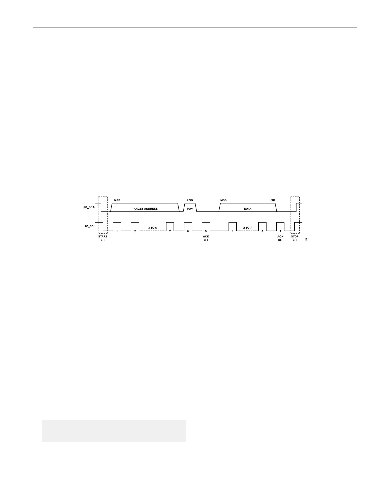
Figure 57 shows a typical I
2
C transfer.
An initiator device can be configured to generate the serial clock.
The frequency is programmed by the user in the serial clock divisor
register, DIV. The initiator channel can be set to operate in fast
mode (400 kHz) or standard mode (100 kHz).
Figure 57. Typical I
2
C Transfer Sequence
The user programs the I
2
C bus peripheral address in the I
2
C bus
system. This ID can be modified any time a transfer is not in
progress. The user can set up to four target addresses that are
recognized by the peripheral. The peripheral is implemented with a
2‑byte FIFO for each transmit and receive shift register. The IRQ
and status bits in the control registers are available to signal to the
processor core when the FIFOs need to be serviced.
I
2
C OPERATION
I
2
C Startup
The following steps are required to run the I
2
C peripheral:
1. Enable PCLK to the I
2
C peripheral by setting CTL5, Bit 5
and CTL5, Bit 3 = 0. PCLK frequency is controlled via CTL1,
Bits[13:8].
2. Configure the digital pins (P0.4/I2C_SCL and P0.5/I2C_SDA)
for I
2
C operation via the GP0CON register.
3. Ensure the drive strength for the P0.4/I2C_SCL pin and P0.5/
I2C_SDA pin is increased to ensure reliable I
2
C communica-
tions, as detailed in the following example code:
GP0DS = 0x30; // Increase drive strength
of I2C pins.
4. Configure the I
2
C registers as required for target or initiator
operation.
5. Enable the I
2
C target or initiator interrupt source as required.
When using I
2
C, the user must disable the internal pull-up resistors
on the I
2
C pins via the GP0POL register. The GPIO multiplexed
configuration mode is I2C_SCL for P0.4/I2C_SCL and is I2C_SDA
for P0.5/I2C_SDA.
7-Bit Addressing
The ID0 register, ID1 register, ID2 register, and ID3 register contain
the target device IDs. The ADuCM356 compares the four IDx
registers to the address byte. To be correctly addressed, the seven
MSBs of IDx registers must be identical to that of the seven MSBs
of the first received address byte. The LSB of the IDx registers
(R/W or the transfer directional bit) is ignored in the process of
address recognition. The initiator addresses a device using the
ADR1 register.
10-Bit Addressing
This feature is enabled by setting SCTL, Bit 1 for initiator and
target mode. The 10-bit address of the target is stored in the
ID0 register and ID1 register, where the ID0 register contains the
first byte of the address, and the R/W bit and the upper five bits
must be programmed to 11110, as shown in Figure 58. The ID1

Table of Contents

Question and Answer IconNeed help?

Do you have a question about the Analog Devices ADuCM356 and is the answer not in the manual?

Analog Devices ADuCM356 Specifications

General IconGeneral
BrandAnalog Devices
ModelADuCM356
CategoryMicrocontrollers
LanguageEnglish

Summary

PREFACE

SCOPE

Provides a detailed description of the functionality and features of the ADuCM356.

CLOCKING ARCHITECTURE

DIGITAL DIE CLOCK FEATURES

Details the clock sources, dividers, and gating for the digital die system clock.

ANALOG DIE CLOCK FEATURES

Details the clock sources, dividers, and gating for the analog die system clock.

POWER MANAGEMENT UNIT

Active Mode

Describes the fully active operating mode where the Arm Cortex-M3 executes from flash and SRAM.

Flexi Mode

Describes the mode where the Arm Cortex-M3 is disabled, allowing peripherals to operate.

Hibernate Mode

Describes the low-power mode where the digital core and most analog blocks are powered down.

SYSTEM RESETS

DIGITAL DIE RESET OPERATION

Explains the reset sources and operation for the digital die, including software resets.

PROGRAMMING, PROTECTION, AND DEBUG

Debug Features

Details the SWD port, flash patch breakpoints, and data watchpoint/trigger units for debugging.

SYSTEM EXCEPTIONS AND PERIPHERAL INTERRUPTS

CORTEX-M3 AND FAULT MANAGEMENT

Describes the system exceptions and fault handling features integrated with the Cortex-M3 processor.

ANALOG DIE CIRCUITRY SUMMARY

ADC, HIGH-SPEED DAC, AND ASSOCIATED AMPLIFIERS OPERATING MODE CONFIGURATION

Configures the operating modes for ADC, High-Speed DAC, and associated amplifiers.

ADC CIRCUIT

ADC CIRCUIT FEATURES

Lists the key features of the ADuCM356's fast multichannel, 16-bit ADC.

LOW-POWER POTENTIOSTAT AMPLIFIERS AND LOW-POWER TIAS

LOW-POWER POTENTIOSTAT AMPLIFIERS

Details the two low-power potentiostat amplifiers for setting external sensor bias voltage.

HIGH-SPEED DAC CIRCUITS

HIGH-SPEED DAC OUTPUT SIGNAL GENERATION

Explains how to generate high-speed DAC output voltage via direct write or waveform generator.

PROGRAMMABLE SWITCHES CONNECTING THE EXTERNAL SENSOR TO THE HIGH-SPEED DAC AND HIGH-SPEED TIA

DX SWITCHES

Selects pins for the high-speed DAC excitation amplifier output, used for impedance measurements.

SEQUENCER

SEQUENCER COMMANDS

Describes the two types of commands: write commands and timer commands (wait, timeout).

SLEEP AND WAKE-UP TIMER

CONFIGURING A DEFINED SEQUENCE ORDER

Defines the order of sequence execution periodically using the SEQORDER register.

USE CASE CONFIGURATIONS

HIBERNATE MODE WHILE MAINTAINING A DC BIAS TO THE SENSOR

Details setup for hibernate mode while maintaining sensor bias voltage.

DMA CONTROLLER

DMA FEATURES

Lists the features of the ADuCM356's dedicated and independent DMA channels.

FLASH CONTROLLER

SUPPORTED COMMANDS

Summarizes the commands supported by the flash controller for read, write, erase, and signature operations.

REGISTER DETAILS: FLASH CACHE CONTROLLER (FLCC)

COMMAND REGISTER

Allows execution of specified flash commands like write, erase, abort, and signature generation.

DIGITAL INPUTS AND OUTPUTS

DIGITAL INPUTS AND OUTPUTS OPERATION

Explains how to configure, read, and write digital input and output pins.

I2C SERIAL INTERFACE

I2C OPERATION

Details the steps required to run the I2C peripheral, including startup and modes.

SERIAL PERIPHERAL INTERFACES

SPI OPERATION

Describes the operation of the SPI interface, including initiator and target modes.

REGISTER SUMMARY: SPI0/SPI1

STATUS REGISTERS

Provides status information for SPI0 and SPI1, including ready, overflow, and error conditions.

REGISTER DETAILS: UART

INTERRUPT ENABLE REGISTER

Configures which interrupt sources generate an interrupt for the UART.

DIGITAL DIE GENERAL-PURPOSE TIMERS

GENERAL-PURPOSE TIMER OPERATIONS

Explains the operation of timers in free running mode and periodic mode.

REGISTER SUMMARY: ANALOG DIE GENERAL-PURPOSE TIMERS

CONTROL REGISTER

Controls timer operation, including clock source, mode, and event selection.

REGISTER DETAILS: DIGITAL DIE WAKE-UP TIMER

STATUS 0 REGISTER

Provides status information for WUT operation, including synchronization and pending writes.

CYCLIC REDUNDANCY CHECK

CRC OPERATING MODES

Details the core access and DMA access modes for CRC calculation.

REGISTER SUMMARY: CRC

CRC CONTROL REGISTER

Controls the CRC peripheral, including enabling, mirroring, and calculation order.

HARDWARE DESIGN CONSIDERATIONS

SERIAL WIRE DEBUG INTERFACE

Describes the SWD interface for debugging and programming, replacing JTAG.