Reference Manual ADuCM356
DIGITAL DIE WAKE-UP TIMER
analog.com Rev. A | 288 of 312
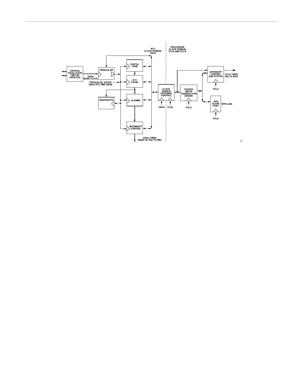
Figure 65. Digital Die WUT Block Diagram
WUT OPERATING MODES
Initial WUT Power-Up
The WUT operates in a dedicated voltage domain that is continu-
ously powered under normal conditions. However, when a battery
is attached for the first time or replaced, a POR occurs. This POR
resets all WUT registers. Upon detecting a WUT failure, the CPU
reprograms the count registers of the timers and clears the fail flag
in the timer control register. The CPU can optionally program the
alarm registers of the timer to generate an interrupt when the alarm
and count values match.
Persistent Sticky Wake-Up Events
When the device is in a power-down mode, there are no losses of
timer alarm events. If the alarm is enabled, the resulting interrupt
is asserted by the WUT so that the NVIC subsequently sees an
RCLK timed version of the interrupt when power is restored to the
processor. To facilitate this interrupt, the timer sends a 32 kHz timed
version of the same interrupt to the wake-up controller in the PMU,
which causes the digital core to be repowered. When the CPU is
woken up, it can inspect both the PMU and WUT to understand the
cause of the interrupt event for the wakeup.
WUT Capacity to Accommodate Posted Writes
by CPU
If a posted write by the CPU to a 32 kHz sourced MMR in the
WUT is pending dispatch in the WUT clock domain due to a queue
of other similar register writes to the 32 kHz domain, a second or
subsequent write by the CPU to the same WUT register cannot be
stacked up to overwrite the pending transaction. Any such attempts
are rejected by the WUT. These result in SR0, Bit 4 interrupt events
in the WUT (see the Status 0 Register section).
Snapshot of the Timer Counter
The CPU can instruct the timer to take a snapshot of its elapsed
time count by writing a software key of 0x7627 to the GWY regis-
ter. This causes the combined three snapshot registers (SNAP0,
SNAP1, and SNAP2) to update to the current value of the three
count registers (CNT0, CNT1, and CNT2) and to maintain this
snapshot until subsequently told by the CPU to overwrite it.
WUT RECOMMENDATIONS: CLOCK AND
POWER
Stopping the PCLK
Before entering any mode that causes the PCLK to stop, the CPU
must first wait until there is confirmation from the WUT that no
previously posted writes have yet to complete. The CPU can check
this by reading both the SR0 and SR2 registers.
Ensuring No Communication Across WUT
Power Boundary When Powering Down
When the CPU has advance knowledge about a power-down, it
must either check to confirm that there are no posted writes in the
WUT awaiting execution or cancel all queued and executing posted
writes in the WUT. Cancellation is achieved by writing a cancellation
key of 0xA2C5 to the GWY register, which takes immediate effect.
These actions maintain the integrity of the always on half of the
WUT.
Do not post any further register writes to the WUT until power is
lost by the core to ensure that no communication between the CPU
and the WUT occurs. Such communication makes the WUT liable
to corruption when the WUT power domains isolation barrier is
subsequently activated.
 Loading...