Reference Manual ADuCM356
CLOCKING ARCHITECTURE
analog.com Rev. A | 13 of 312
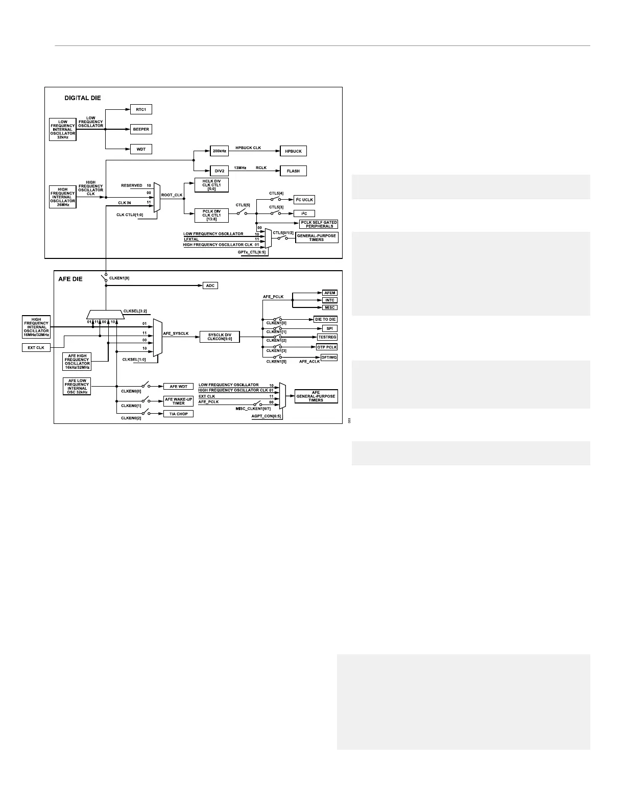
Figure 2. Clock Architecture Block Diagram
CLOCK GATING
In the case of certain clocks, clocks can be individually gated
depending on the power mode or register settings. For more infor-
mation about clock gating and power modes, refer to the Power
Management Unit section.
On the digital die, the clock gates of the peripheral clocks are user-
controllable in certain power modes. Register CTL5 in CLKG0_CLK
can be programmed to turn off certain clocks, depending on the
user application. Set the appropriate bits in the CTL5 register to 1 to
disable the clock to individual blocks.
On the analog die, use the CLKEN0 register and the CLKEN1
register to disable the system clock to different peripherals on the
analog die.
CONNECTING AFE DIE CLOCK TO DIGITAL
DIE CLOCK INPUT
The AFE die 16 MHz oscillator is a more accurate oscillator than
the 26 MHz high frequency oscillator on the digital die. For UART
communications, select the AFE die 16 MHz oscillator as the input
clock to the digital die. Internally, the AFE system clock can be
connected to an internal pad, P2.2, on the AFE. There is an internal
bond wire connecting this AFE die pad to the digital die pad, P1.10,
on the digital die that can be configured as the external clock input
for the digital die.
To connect and select the AFE die 16 MHz oscillator as the external
clock input for the digital die, perform the following steps:
1. Enable AFE die Pad P2.2 as an output.
pADI_AGPIO2->OEN |= 0x4;
2. Configure the internal digital die Pad P1.10 as an input and
configure its mode as EXT_CLKIN.
DioCfgPin(pA►
DI_GPIO1,PIN10,2); //
External Clock mode for Digital die P1.10
DioIenPin(pA►
DI_GPIO1,PIN10,1); //
Enable p1.10 input path
3. Clear CLKEN1, Bits[9:8]. The user is required to close the
switch on the AFE die to connect the AFE die clock to the P2.2
pad.
pADI_AFECON->CLKEN1 &=
0x0FF; // Clear
CLKEN1 bits 9:8
4. Select the digital die clock source as the external clock from the
AFE die.
DigClkSel(DIGCLK_SOURCE_AFE);
If the clock source is a 32 MHz external crystal, ensure the
clock to the digital die is 16 MHz by setting CLKCON[9:6] = 2.
Hibernate Mode and AFE Die Clock Selected
on Digital Die
Switch the digital die clock source back to a digital die clock before
entering hibernate mode. The device does not wake up if both dice
are in hibernate mode and the AFE die clock is used by both dice,
because, on waking from hibernate mode, the digital die wakes
first. The digital die then must read or write to an AFE die register
to wake the AFE die. If the AFE die is the clock source to both dice,
the wake-up sequence does not complete.
To enter hibernate mode, use the following suggested sequence:
DigClkSel(DIGCLK_SOURCE_HFOSC); //
Switch digital die clock back to its own oscil►
lator
pADI_UART0->COMDIV = 0; // Clear
COMDIV to ensure UART operates after wake-up
EnterHibernateMode(); // Enter
Hibernate mode
 Loading...