Reference Manual ADuCM356
SEQUENCER
analog.com Rev. A | 130 of 312
is enabled. If conflicts arise, the sequencer has the priority. If the
sequencer and the processor write at the same time, the host
controller is ignored. There is no error report for this conflict. Do not
write to a register when the sequencer is running. However, there
are registers that are exceptions and can be written to freely without
any conflict. The SEQCON register allows ending a sequence
execution (SEQEN bit) and halting a sequence (SEQHALT bit).
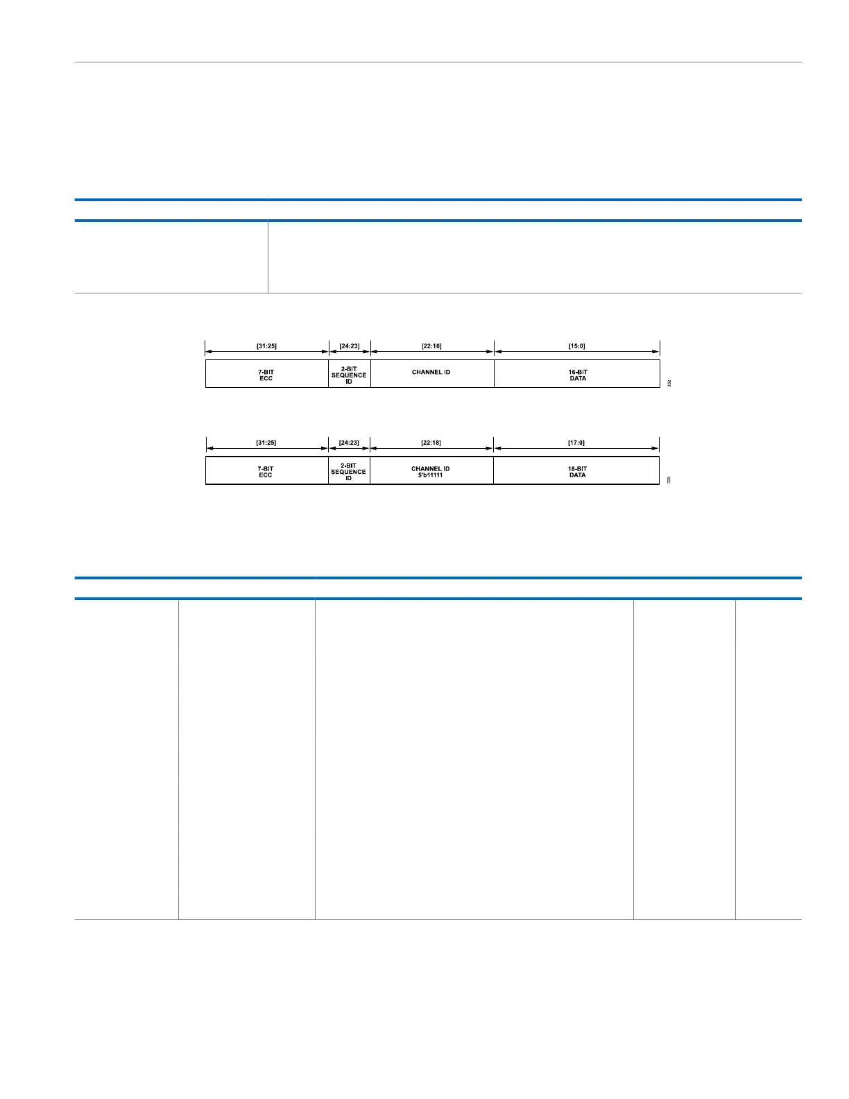
Table 153. Channel ID Description
Data FIFO Word, Bits[22:16] Description
11111XX
1
DFT result
11110XX Mean from statistics block
1XXXXXX Sinc2 filter result, XXXXXX is the ADC multiplexer positive setting (ADCCON register, Bits[5:0])
0XXXXXX Sinc3 filter result, XXXXXX is the ADC multiplexer positive setting (ADCCON register, Bits[5:0])
1
X means don’t care.
Figure 32. Data FIFO Word Format
Figure 33. Data FIFO DFT Word Format
SEQUENCER AND FIFO REGISTERS
Table 154. Sequence and FIFO Registers Summary
Address Name Description Reset Access
0x400C2004 SEQCON Sequencer configuration register 0x00000002 R/W
0x400C2008 FIFOCON FIFO configuration register 0x00001010 R/W
0x400C2060 SEQCRC Sequencer CRC value register 0x00000001 R
0x400C2064 SEQCNT Sequencer command count register 0x00000000 R/W
0x400C2068 SEQTIMEOUT Sequencer timeout counter register 0x00000000 R
0x400C206C DATAFIFORD Data FIFO read register 0x00000000 R
0x400C2070 CMDFIFOWRITE Command FIFO write register 0x00000000 W
0x400C2118 SEQSLPLOCK Sequencer sleep control lock register 0x00000000 R/W
0x400C211C SEQTRGSLP Sequencer trigger sleep register 0x00000000 R/W
0x400C21CC SEQ0INFO Sequence 0 information register 0x00000000 R/W
0x400C21D0 SEQ2INFO Sequence 2 information register 0x00000000 R/W
0x400C21D4 CMDFIFOWADDR Command FIFO write address register 0x00000000 R/W
0x400C21D8 CMDDATACON Command data control register 0x00000410 R/W
0x400C21E0 DATAFIFOTHRES Data FIFO threshold register 0x00000000 R/W
0x400C21E4 SEQ3INFO Sequence 3 information register 0x00000000 R/W
0x400C21E8 SEQ1INFO Sequence 1 information register 0x00000000 R/W
0x400C2200 FIFOCNTSTA Command and data FIFO internal data count register 0x00000000 R
0x400C0430 TRIGSEQ Trigger sequence register 0x0000 R/WS
Sequencer Configuration Register
Address: 0x400C2004, Reset: 0x00000002, Name: SEQCON
 Loading...