Reference Manual ADuCM356
LOW-POWER POTENTIOSTAT AMPLIFIERS AND LOW-POWER TIAS
analog.com Rev. A | 81 of 312
The ADuCM356 features two low-power TIAs and two low-power
potentiostat amplifiers. This section details the operation of these
components.
LOW-POWER POTENTIOSTAT AMPLIFIERS
The ADuCM356 has two low-power potentiostat amplifiers de-
signed to set the bias voltage of an external electrochemical sen-
sor. The bias voltage is the voltage between the sense electrode
and reference electrode. Depending on the electrochemical sensor
used, a specific bias voltage is required. The bias voltage is set
by the low-powers DACs. See the Low-Power DACs section for
details.
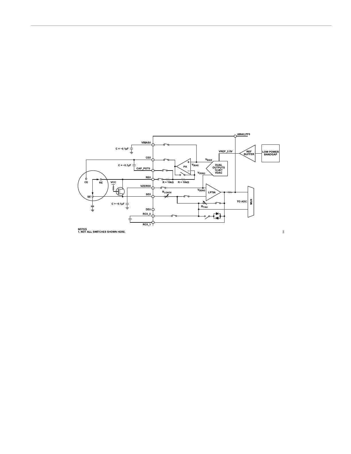
Figure 15 shows the potentiostat amplifier connected to a 3-lead
electrochemical sensor. The potentiostat amplifier (labeled PA in
Figure 15) has the V
BIAS
output of the dual DAC as its noninverting
input. The amplifier output is connected to the counter electrode.
The reference electrode is connected to the inverting input of the
potentiostat. As such, the voltage on the reference electrode is
determined by the V
BIAS
DAC output voltage via the potentiostat
amplifier.
Figure 15. Low-Power Potentiostat and Low-Power TIA and DAC Connected to One Electrochemical Sensor
LOW-POWER TIAS
Two low-power TIA channels are available on the ADuCM356.
The load resistor and gain resistor values are specified in the Lx
registers. Select the TIA gain resistor that maximizes the ADC input
voltage range for the selected PGA gain setting. For example, if
the PGA gain setting is 1, select a TIA gain resistor to maximize
the ±900 mV range. To calculate the required gain resistor, use the
following equation:
I
MAX
= 0.9/R
TIA
(6)
where:
I
MAX
is the expected full-scale input current.
R
TIA
is the TIA gain resistor selected by LPTIACONx, Bits[9:5].
A number of operation modes are selectable by user code. The dif-
ferent modes are selected by configuring a series of switches. Fig-
ure 16 shows the various switches for Channel 0. These switches
are controlled within the LPTIASW0 register. The switches in Figure
17 are controlled by the LPTIASW1 register for Channel 1. Switch
0 (SW0) to Switch 13 (SW13) are the same for both channels.
Channel 1 does not have SW15 or SW14. The LPTIASW0 register,
Bit 0, controls SW0, and the LPTIASW0 register, Bit 1, controls
SW1.
Low-Power TIA Protection Diodes
Figure 16 shows back to back protection diodes connected parallel
to the R
TIA0
gain resistor. These diodes can be connected or
disconnected by controlling SW0, which in turn is controlled by
LPTIASWx, Bit 0. These diodes are intended for use when switch-
ing R
TIA
gain settings to amplify small currents to prevent saturation
of the TIA. These diodes have a leakage current specification that
is dependent on the voltage across them. The leakage current is
large if the differential voltage across the diode is >200 mV. The
leakage current can be >1 nA and several microamperes if >500
mV.
Close SW0 when changing the R
TIA
value, and open SW0 again
when the change is complete. If high currents are detected on the
low-power TIA input path when using an oxygen electrochemical
sensor, close the shorting switch, SW1, to protect the low-power
TIA input circuitry. SW1 is controlled by LPTIASWx, Bit 1. For full
details of the high-speed TIA in Figure 16 and Figure 17, refer to
the High-Speed TIA Circuits section.
 Loading...