Circuit Pack Descriptions
Issue 8.0 July 2002
7-55
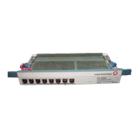
In the transmit direction (toward the OC-48 line), the OC3 (1.3 STD) circuit pack
accepts one OC-3 (155.52 Mb/s) non-return-to-zero (NRZ) synchronous optical
network (SONET) compatible optical signal. Fiber access to the OC3 (1.3 STD)
circuit pack is via a fixed
ST
â
-type buildout block and a removable
ST
-type,
FC/PC-type, or SC-type lightguide buildout on the circuit pack faceplate (labeled
IN). Lightguide buildouts are chosen based on the attenuation desired, the type of
connector interface, and the type of lightguide jumpers (single-mode or
multimode). All factory-equipped OC3 (1.3 STD) circuit packs come with a
removable
ST
-type 0-dB lightguide buildout. When installing or removing
lightguide buildouts, do not pull the beam (front tab) outward. Pulling the beam
(front tab) outward could result in breaking the beam (front tab).
The optical-to-electrical module receives the OC-3 signal, converts it to an
electrical STS-3/3c signal (155.52 Mb/s), and sends it to a timing recovery circuit.
The timing recovery circuit recovers a 155.52 MHz clock signal from the STS-3/3c
signal and retimes the STS-3/3c signal with the recovered clock signal. The
STS-3/3c and clock signals are then sent to the OC-3 line STS-3 byte processor.
The OC-3 line STS-3 byte processor descrambles and demultiplexes the
STS-3/3c signal into three STS-1 signals (51.84 Mb/s) and outputs the three
STS-1 signals and a common clock signal to the transmit pointer processor.
The transmit pointer processor performs frequency adjustment and pointer
processing on the three received STS-1 signals. This synchronizes the STS-1
signals to the 51.84 MHz system clock. The 51.84 MHz clock signal is obtained by
dividing the 155.52 MHz from the Timing Generator, Stratum 3 - DS1 [TG3 (DS1)]
circuit packs by three. The divide-by-three circuit is part of the low speed STS-3
byte processor. The three STS-1 signals are then sent to the low speed STS-3
byte processor.
The low speed STS-3 byte processor scrambles and multiplexes the three STS-1
signals back to one STS-3/3c signal (155.52 Mb/s). The high speed interface
distributes the STS-3/3c signal to the OC48 TRMTR circuit packs.
Receive Direction. 7In the receive direction (toward the OC-3 line), the high speed
interface of a LAA10 OC-3 circuit pack accepts an STS-3/3c signal (155.52 Mb/s)
from one of the OC48 RCVR circuit packs and sends it to a timing recovery circuit.
The timing recovery circuit recovers a 155.52 MHz clock signal from the STS-3/3c
signal and retimes the STS-3/3c signal with the recovered clock signal.
In the receive direction (toward the OC-3 line), the high-speed interface of a
LAA10B OC-3 circuit pack accepts two STS-3/3c signals (155.52 Mb/s) from both
of the OC48 RCVR circuit packs and sends them to two timing recovery circuits.
The timing recovery circuits recover a 155.52 MHz clock signal from each
STS-3/3c signal and retime the STS-3/3c signals with the recovered clock signals.
The two retimed STS-3/3c signals are then demultiplexed into six STS-1 signals.
Three of these STS-1 signals are chosen depending on system provisioning and
multiplexed into a STS-3/3c signal.
The STS-3/3c signal and clock signals are then sent to the low-speed STS-3 byte
processor. The low-speed STS-3 byte processor descrambles and demultiplexes